
Low Noise Power Supply [240386]
Fully analog adjustable medium power symmetrical power supply without any switching or digital parts. 0 – 22 V output voltage, 0 – 1 A output current.
Interested in a kit of parts for this project?
Back this project on its JumpStarter page!
Back this project on its JumpStarter page!
Back this project on its JumpStarter page!
Design considerations
Most laboratory power supplies and AC adapters these days are switched mode types. Even the best of them still have a high frequency ripple and other artifacts present on the output voltage, inherent to their design. When testing sensitive analog circuits this can cause problems, interfere with low level measurements. So, why not design a fully analog power supply. Of course efficiency is less, but for testing purposes this is not an issue and ensures results are more reliable.
Since many analog circuits require a symmetrical supply voltage, this power supply has to have a symmetrical output voltage. The positive and negative output voltage have equal levels, with a limited adjustment to compensate any imbalance. Of course a variable current limit is also a requirement.
The first idea was to place both power transistors of the output stages on a common heat sink and use a single mains transformer with two equal secondary windings. However, design requirements are an adjustable output voltage of 0 to +/- 22 V and an adjustable current limit of 0 to +/- 1 A. In this setup a standard mains transformer with 2 x 22 V secondary voltages would be a good candidate to provide the source voltage for the regulator stages. However at a (permanent) short circuit condition with both outputs set to maximum current almost 60 W must be dissipated. To limit the temperature rise to 30 °C the thermal resistance of the heat sink must be approximately 0.5 °C/W. That’s a large heatsink. To limit the size of the heatsink to a minimum the input voltage of the regulators would have to be proportional to the output voltage. Taking in to account voltage drop across the rectifiers and inductors of the filters and fuse, ripple voltage across the smoothing capacitors and drop-out voltage of the regulator the input voltage would have be at least 3,5 V higher than the output voltage. Only a switched mode circuit or something similar could resolve this and of course no option here. Less perfect but still a good alternative is to use more than one secondary voltage and select a higher AC voltage in discrete steps when needed. Two AC voltages is a minimum but three is better and will reduce the size of the heat sink considerably. Even more so by using two heat sinks, one per output stage. The heat sinks are now small PCB mounted versions and as an additional advantage make the construction a lot easier. In a worst case scenario at 30 V input voltage and 1 A short circuit current, the power of 30 W would cause a temperature rise of 81 °C in the 2.7 °C/W heat sinks. The junction of the power transistor would still be lower than its specified maximum of 150 °C. But consider this, when the junction of a transistor is hotter than 70 °C for a prolonged time, this will reduce its lifespan. To protect against such an excessive temperature rise a thermal switch could be considered, not used here. Types exist that can switch mains voltages.
Instead of a single custom transformer with 6 secondary windings three identical transformers are used. The toroidal transformers are encapsulated PCB mounted versions and a separate PCB is designed (240386-3). This also makes the construction easier, the relay circuit to select the correct AC voltage is placed on this PCB and it can be mounted at some distance from the regulator PCB.
Noise from the mains voltage is reduced by a separate common mode filter with two common mode chokes, a smaller third PCB (240386-2).
To keep the design completely analog instead of digital panel meters 4 small moving coil meters indicate both output voltage and current of each regulator. Advantage of the moving coil meters is they don’t need an additional power supply. Accuracy and resolution is perhaps a bit lacking. But good practice is to use a multimeter to check the output voltage and current of any power supply. The connection of the current meter is placed inside the feedback loop of the output stage. This way its resistance has no influence on the output voltage.
Two window comparators (quad comparator IC8) select the AC input voltage needed for the regulators, one per output voltage. In case one of the current limits is active the highest output voltage determines the AC volage. Downside of this choice is the heat sink of the limiting output will get hotter because of the higher voltage drop across the power transistor. This is a choice to reduce the size of the regulator, not making it too complex.. Otherwise two AC inputs and rectifiers would be needed and would make the power supply more like two separate ones.
Higher efficiency could be achieved by using Ideal Diode Bridge Controller LT4320 for the rectifier. But it doesn’t work with a center tap transformer design to create symmetrical DC voltages. Two ICs would be needed with each 4 MOSFETs. That’s a bit extreme. So, to ensure a low as possible voltage drop a standard diode bridge with Schottky rectifiers is used. The V30100CI-M3/P contains two diodes in a TO-220 package, these are connected in parallel to lower the voltage drop across the rectifiers a little more.
Initially rail-to-rail-in-out opamps are used so only a single supply voltage per regulator is required, making the PCB design less complex. While testing an earlier concept a LT1677CN8 was used in a non inverting setup for the regulators. Depending on voltage rise of the supply voltages and input levels during this time the output of the opamp was locked to a low level, although input levels were well within its specifications when the power supply was settled. Extra input protection diodes solved it, the internal input protection diodes apparently are not preventing this problem. It has a very high absolute maximum supply voltage of 44 V and overall very good specifications. Ideal since it is directly connected to the rectified AC voltage. But its input bias current and limited differential input voltage, use as a true comparator is not possible, made it necessary to look for an alternative. The current control of the regulators uses one of the amplifiers as a comparator. The OPAx992 family was chosen. The maximum differential input voltage range is the supply voltage and input bias current is only ±1- pA. Also offset voltage, offset voltage drift and input noise are extremely low. Downside of newly developed opamps is the availability in SMD packages only. The PCB uses dual footprints for the single and dual versions of the opamps. This makes measurements easier and safer. The pads of the DIP footprint make it less likely a short circuits occurs by slipping of a probe. Sadly this is not possible with the quad version in any easy way. When measuring the pins of the quad versions be careful and measure a connected component instead of the lead of the IC itself.
Output current of each regulator is measured across a shunt in the output of the regulator. If the power supply was a single version the shunt could be placed in the ground terminal. But since there is a common ground here this is not possible. A differential amplifier is required to subtract the common mode voltage, which is in fact the output voltage. To increase the precision of the measured voltage across the shunt the tolerance of the 4 resistors needs to be 0.1 %.
Depending on the level of the common mode input voltage of rail-to rail opamps specifications can vary. Often there’s a small range where the complementary differential input pairs are both active and some specifications are different. This region is close to one a the supply rails. To avoid this the regulators were changed to an inverting topology. This ensures both inputs of the opamps controlling the output voltage are always at ground level.
Interested in a kit of parts for this project?
Back this project on its JumpStarter page!
A positive refence voltage is created directly from the filtered and rectified AC voltage. To ensure a clean reference voltage a Precision Micropower Shunt Voltage Reference LM4040 is used. Its operating current is provided by Adjustable Current Source LM334 and is approximately 4.6 mA. 1 mA is flowing into P1 and P3. The combination of a current source and voltage reference suppresses any noise and interferences coming from the unregulated source voltage. The level of this rectified AC voltage depends on the output voltage of the regulators. The current source also keeps the operating current of the LM4040 independent of the input voltage. Both reference and current source are still available in a TO-92 package. The reference is also available in a SOT-23 package. The footprint combines both packages. This way also a newer LM4050 can be used, but the latter has a higher wide band noise than the LM4040, 93 µV instead of 80 µV (10 Hz to 10 kHz at 100 µA). This positive reference voltage is connected to the potentiometer (P1) that controls the level of both output voltages. Its wiper is buffered to create the positive control voltage -Vset for the negative regulator. An extra inverter is used to create the negative control voltage +Vset for the positive regulator. The gain of this amplifier is slightly adjustable (P2) to compensate for any difference in absolute voltage levels of the regulators. Current limit setting is the same for both regulators but independent of each other. Three single potentiometers are necessary and either single turn of multiturn potentiometers can be used, the latter being more expensive of course.
As said before, the intention to use rail-to-rail opamps was a simpler design. But several reasons made it necessary to use additional supply voltages, a low negative supply voltage for the positive regulator circuit and a low positive supply voltage for the negative regulator circuit. To create these two supply voltages a LM317 and LM337 were added. Connecting their adjust to ground creates +1.25 V and – 1.25 V. Rail-to rail sounds nice but in practice the output voltages are never equal to the supply rails. The residual voltage are the cause setting the current limit to 0 A was not 0. Two extra trimmers were added to compensate this partially. The two additional regulated supply voltages are also the reference voltages for these trimmers.
To filter any residual interferences from the transformer PCB a common mode filter and differential mode filters are added to filter the rectified voltages.
To prevent output voltages rise above the set values when the power supply is shut down a relay short circuits the drive of both output stages. The relay is powered by an isolated rectifier, connected separately to the transformer PCB, and a small smoothing capacitor to deactivate the relay instantly when the power supply is turned off. The relay also speeds ups the discharging of the (additional) capacitors connected to the outputs of the regulators through R19 and R44.
Mains filter
Mains voltages contain all kinds of noise and interferences. To use the mains voltage as a source for a low noise power supply it first has to be filtered. In most cases common mode interference is worse than differential mode interference, latter can often be filtered by a simple low pass RC filter or better yet an LC filter. To increase the suppression of these common mode signals instead of a single common mode choke two are used.

Fig. 1. Mains filter for the Low Noise Power Supply (240386-2 v2.1).
The schematic is standard. The capacitors C3…C6, connected from the mains voltage to ground are of type Y. The capacitors C1 and C2, connected between the mains voltage, are type X. The fuse is rated 500 mA when a mains voltage of 230 VAC is used, and 1 A in case of 115 VAC. The value depends on three times the primary fuse rating of the three mains transformers of the Low Noise PSU. Metal Oxide Varistor MOV1 protects against large voltage spikes. For 115VAC the S14K300 (ordering code B72214S0301K101) should be replaced by type S14K150 (ordering code B72214S0151K101). Resistor R1 discharges the capacitors when the filter is disconnected from the mains, should no load be connected to K2. K2 must be connected to K1 on transformer PCB 240386-3.
Construction mains filter PCB (240386-2 v2.0)
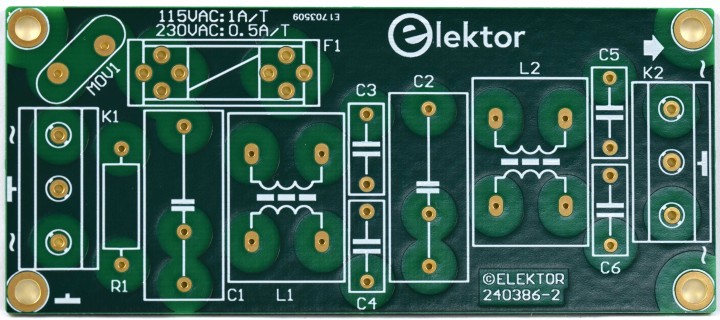
Fig. 2. PCB for the mains filter (240386-2 v2.0).
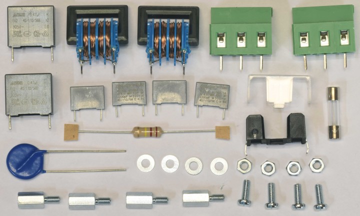
Fig. 3. All parts for the mains filter PCB (240386-2 v2.1).
Start by soldering de lowest components. Resistor R1 first and the common mode chokes L1 and L2 last.
Proposed order:
Resistor R1
Capacitors C3, C4, C5, C6
Fuse holder F1
Varistor MOV1
Capacitors C1, C2
Screw terminal blocks K1, K2
Common mode chokes L1, L2
Insert the fuse (500 mA T for 230 VAC or 1 A T for 115 VAC)
Place the cover for the fuse holder
Mounting of 4 standoffs can wait until an enclosure is constructed/adapted
The mains filter is now ready for use
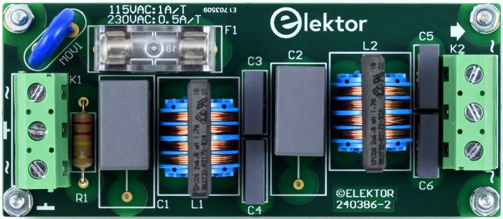
Fig. 4. All parts fully mounted and soldered and the filter is ready for use.
Bill of materials PCB 240386-2 v2.1
Resistor
R1 = 220 kΩ, 1 W, 500V, 5 %
Capacitor
C1, C2 = 470 nF, 305 VAC, Class X2, 11x27 mm max., LS 15/22.5 mm
C3, C4, C5, C6 = 2.2 nF, 300VAC, Class Y2, 13x4 mm, LS 10 mm, PP
Inductor
L1, L2 = Common mode choke, 6.8 mH, 1.7 A, TDK B82732R2172B030
Semiconductor
MOV1 = TVS varistor, 300VAC S14K300
Other
K1, K2 = 3way screw terminal block, LS 7.62 mm
F1 = 0.5 A time delay, 250V, cartridge fuse 5 x 20 mm
F1 = 1 A time-lag, 250V, cartridge fuse 5 x 20 mm
F1 = Fuse holder 5x20 mm, 10 A, 500 VAC
F1 = Cover for fuse holder, transparent
4 x10 mm M3 standoff, steel, male-female
4 x M3 screw, 8 mm, steel, pan head
4 x M3 nut
Interested in a kit of parts for this project?
Back this project on its JumpStarter page!
Transformers
To keep the heat sink of each output stage of the two voltage regulators as small as possible, so types that can be mounted on the PCB can be used, the AC input voltage of the regulator is divided in three levels. This also improves overall efficiency. Two relays are controlled by the regulator to select the correct AC voltage, depending on the DC output voltage. Two optocouplers make sure there’s no ground loop between the AC input voltage of the regulators and the power ground of the relay coils. The MOC8021M has a very high current transfer ratio, minimum 1000 %.
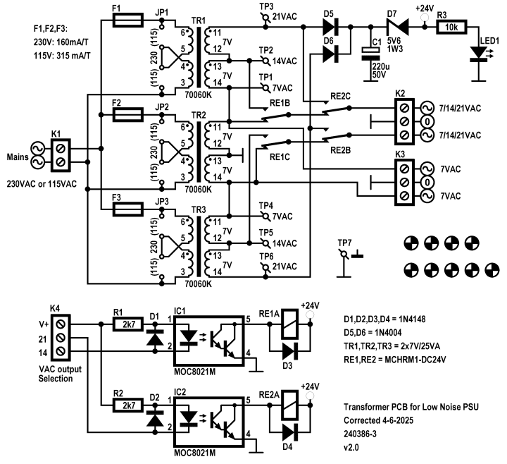
Fig.5. Circuit with the 3 transformers for the Low Noise PSU.
The transformer chosen for the regulator has two separate symmetrical secondary windings. The two secondary windings of TR2 are connected and this is the GND connection of the outputs (K2 and K3). The two secondary windings of TR2 and TR3 are also connected and each transformer is connected to one of the secondary windings of TR1. This way 2x 7, 14 and 21 VAC with counterphase are available on K2. If RE1 and RE2 are turned off 2 x 7 VAC is selected. 2 x 14 VAC is selected if RE1 is turned on and RE2 is still turned off. If RE2 is turned on the output is 2 x 21 VAC independent of RE1. K3 is added to detect turning off the PSU or the sudden absence of the AC voltage on K2 to get the output of the PSU to 0 V as fast as possible. To power the relays the 2 x 21 VAC is rectified by D5, D6 and C1. D7 lowers this voltage to approximately 24 V, the nominal coil voltage of both relays. This voltage varies with current demand of the regulators. D3 and D4 limit the induction spike when the relays are turned off to protect the optocouplers. D1 and D2 prevent potential damage to the LEDs of the optocouplers caused by wrong polarity, for instance in case of faulty wiring.
The chosen transformer also has two separate symmetrical primary windings. These should be connected in series for 230 VAC mains voltage and in parallel for 115 VAC. The primary windings of each transformer are connected to 4 solder pads forming a jumper. 1 jumper wire must be placed for 230 VAC and 2 different jumper wires for 115 VAC.
LED1 can serve as a general POWER ON indicator on the front of the enclosure.
Construction transformer PCB (240386-3 v2.0)
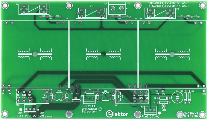
Fig. 6. PCB for the 3 transformers and the surrounding components (240386-3 v2.0).
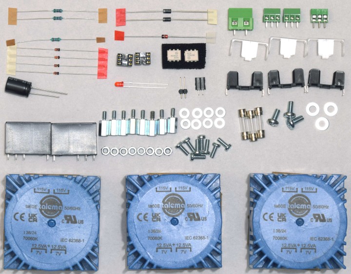
Fig. 7. All Parts for the transformer PCB (240386-1 v2.0).
Start by soldering de lowest components. Jumper wires first and transformers last.
Proposed order:
Jumper wires JP1, JP2 and JP3: 1 for 230 VAC per transformer, 2 for 115 VAC per transformer
Resistors R1,R2 and R3
Diodes D1, D2, D3 and D4
Diodes D5 and D6
Diode D7
DIP-6 IC sockets for optocouplers IC1 and IC2
Screw terminal blocks K2, K3 and K4 (K2 is the different one!)
Pin header for LED1
Fuse holders F1, F2 and F3
Insert the fuses (3 x 160 mA T for 230 VAC or 3 x 315 mA T for 115 VAC)
Place the covers for the fuse holders
Screw terminal block K1
Capacitor C1
Relays RE1 and RE2
Place the three transformers and fasten each with a 8 mm M4 screw and plane washer, only then solder the pins. Be careful when turning the screws inside the thread of the transformers, avoid applying excessive force! This could damage the M4 thread inside the transformers.
Insert optocouplers IC1 and IC2
Optional: LED1 can directly be soldered to the PCB or connected by thin stranded wire and a 2way pin header and socket, since it’s meant to serve as the power indication on the front of the enclosure.
Mounting of the 8 standoffs can wait until an enclosure is adapted/constructed
The transformer PCB is now ready for use.
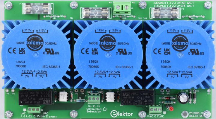
Fig 8. All parts fully mounted and soldered and ready for use.

Fig. 9. Detailed view. Before soldering each transformer is fastened first to the PCB by a 8 mm long M4 screw.
Two side view photos:
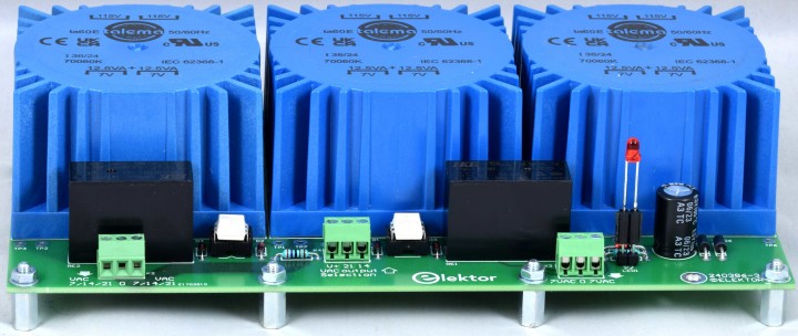
Fig. 10. All parts mounted and soldered. Side view on the low voltage side.
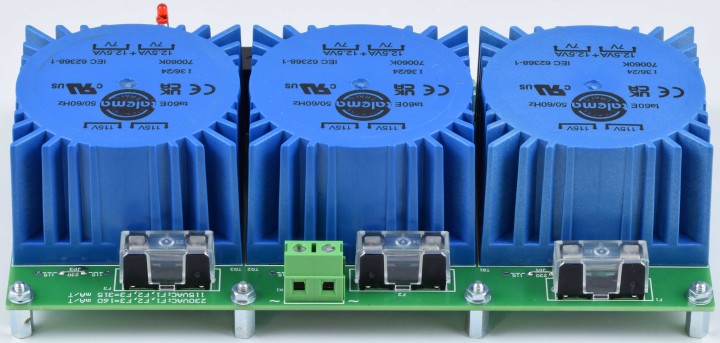
Fig.11. All parts mounted and soldered. Side view on the mains voltage side.
Regarding the transformer PCB:
The transformer PCB is necessary to keep the power loss as low as possible. Design requirements are a symmetrical adjustable output voltage of 0 to 2 x 22 VDC with a common ground and an adjustable output current from 0 to 1 ADC (current limit). If a standard AC voltage of 2 x 22 VAC were to be used, at very low output voltages or sustained short circuit at both outputs and maximum output current, the maximum power loss would be around 60 W. A very large (common) heatsink would be needed and make it an inefficient design. Of coarse this in inherent to an analog PSU. But, by dividing the input voltage of the regulator in 3 levels, these depend on the output voltage, the power loss can be significantly reduced. A separate heatsink for each regulator instead of a very large common one makes the required heatsinks even smaller. Using three separate standard transformers prevents having to use a custom designed transformer with 6 secondary windings.
The PCB can be used with 230 VAC (50 Hz) and 115 VAC (60 Hz) mains voltages. Each transformer has two equal primary windings. For use with 230 VAC these must connected in series. This requires one jumper wire at position 230 next to each transformer. To use the transformer with 115 V AC the two primary windings must be connected in parallel. This requires two jumper wires at positions 115 next to each transformer. Each transformer is protected by a primary fuse of type time delay (also called slow acting), 160 mA for 230 VAC and 315 mA slow acting for 115 VAC.
Bill of materials PCB 240386-3 v2.0
Resistor
R1, R2 = 2.7 kΩ, 600 mW, 1 %
R3 = 10.0 kΩ, 600 mW, 1 %
Capacitor
C1 = 220 uF, 50 V, 20 %, D 10 mm, LS 5 mm, 4000 hours @ 105C
Transformer
TR1, TR2, TR3 = 2x 7 V, 25 VA, PCB mounted toroid, 70060K Talema
Semiconductor
D1, D2, D3, D4 = 1N4148, DO-35
D5, D6 = 1N4004, DO-41
D7 = Zener 5.6 V, 1.3 W, DO-41
LED1 = LED, red, T-1 (3 mm)
IC1, IC2 = MOC8021M, CTR 1000 % min., DIP-6
Other
K1 = 2way screw terminal block, LS 7.62 mm
K2 = 3way screw terminal block, LS 3.5 mm, max. 1.5 mm²
K3, K4 = 3way screw terminal block, LS 3.5 mm, max. 1 mm²
LED1 = Pin header, 1x2, vertical, pitch 2.54 mm
LED1 = Pin socket, 1x2, vertical. pitch 2.54 mm
F1, F2, F3 = Fuse holder 5x20 mm, 10 A, 500 VAC
F1, F2, F3 = Cover for fuse holder, transparent
F1, F2, F3 = 160 mA, time delay, cartridge fuse 5x20 mm
F1, F2, F3 = 315 mA, time delay, cartridge fuse 5x20 mm
RE1, RE2 = Relay DPDT, 5 A/250 VAC/24 VDC,
TR1, TR2, TR3 = M4 screw, 8 mm, pan head
TR1, TR2, TR3 = M4 washer, plain, steel
10 mm M3 standoff, steel, male-female
8 x M3 screw, 8 mm, steel, pan head
8 x M3 nut
8 x M3 washer, plain, steel
IC1, IC2 = IC socket, DIP, 6 contacts
Interested in a kit of parts for this project?
Back this project on its JumpStarter page!
The Regulator
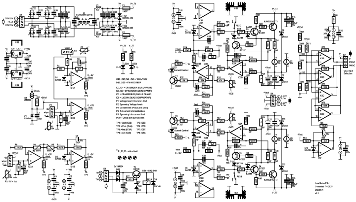
Fig. 12. Schematic of the Low Noise Power Supply (240386-1 v2.1).
The AC voltages from the transformers are rectified by Schottky rectifiers D20…D23 and turned into unregulated DC voltages by smoothing capacitors C46…C49. Ceramic capacitors C50…C53 attenuate 50 Hz (60 Hz) harmonics, caused by switching off of the diodes, and smooth the ripple voltages somewhat. Any common mode interference is suppressed by L3 and C44 and C45. Any differential interference is suppressed by L1/C38/C40/C41 and L2/C39/C42/C43. Additional smoothing capacitors C38…C43 reduce the ripple voltages even more. To protect the opamps, which are all connected to unregulated voltages V+ and V-, transient suppressor diodes TVS1 and TVS2 limit any spikes. V+ and V- are connected to the regulator output stages by 1.6 A fast acting fuses, just to make sure. But, the hardware current limit of approximately 1.2 A in the output stage and the 1 A current control limit of the regulator make it highly unlikely this fuse will ever blow. One situation is possible perhaps, when at the output a higher return voltage from the external load is present. The protection diodes in the output stage would connect this voltage via the fuse to the TVS and the fuse will blow.
Current source IC1 is set to 5.6 mA by R1: Iset (227µV/°K)/Rset = (227*10-6 *298) / 12 = 5.64 mA (at 25 °C, Rset is 12 Ω). The operation current of the reference is 1 mA less, since 10 kΩ potentiometers P1 and P3 are directly connected to IC2 through 3way screw terminal blocks (called P1 and P3). P1 controls both output voltages of the regulators. R2 connects the input of buffer IC3B to ground in case the wiper of P1 makes poor contact or P1 is missing. C2 reduces noise from P1 but also averages a possible unstable voltage when turning P1, caused by bouncing of the wiper. The output of buffer IC3B is the control voltage for the negative regulator and is the reason it’s called -Vset, even if the polarity is positive (0…+5V). The control voltage +Vset is the inverted of -Vset. This is the function of inverting amplifier IC4A. The tolerances of resistors and offsets and offset drift of the opamps can be compensated by varying the gain of IC4A a little. Resistor R6 is connected to the wiper of P2, which is connected to IC4A through a 3way screw terminal block (called P2). In the end positions of P2 R6 is placed in parallel to feedback resistor R4 or R5. The gain of IC4A varies from -0.955 to -1.047, more than ± 4 %. P2 is not intended as a secondary or “fine” adjust for the positive regulator. C6 reduces noise from IC3B and the feedback resistors R4 an R5. If a minor deviation between absolute levels of the regulators is not considered a problem then P2 is optional, not needed. At maximum gain of IC4A and maximum setting of P1 the output voltage of the regulator would be 1.047 * 5 * 4.42 = 23.14 V. At 1 A the regulator will be close to its absolute maximum possible. Depending on the mains voltage the regulator will be close to dropout or possibly beyond. Schottky diode D1 protects the inverting input IC4A from a too high positive voltage in the case the negative supply voltage V- of IC4 is missing.
Getting a little ahead of things. To set the current limit the regulator compares the voltage across a shunt to an adjustable voltage, set by potentiometer P3. The maximum output current is 1A at a voltage of 5 V, the reference voltage delivered by IC2. P3 is buffered by IC3A. To make sure the output is at least 1 A maximal the gain of IC3 A can be increased from 1 to 1.05 by trimmer P4. The current control voltage +Iset for the positive regulator is a positive voltage of 0 to + 5 V. The absolute levels of the current control of both regulators are the same so +Iset is only inverted by IC4B to produce -Iset. The gain of IC4B can be calibrated to exactly -1 by trimmer P5. C7 reduces noise from IC3A and IC4 Band the feedback resistors R11 an R12. Since both opamps of IC3 have a positive output voltage its positive supply is connected to V+ which is still high enough for a stable +5 V when the AC voltage to the rectifiers D20…D23 is 7 V. To ensure the output can be exactly 0V the negative supply voltage of IC3 is -1.25 V. The same is true for IC4. Both of its opamps only have a negative output voltage and its negative supply is connected to V-. Its positive supply is connected to +1.25 V to ensure the outputs can be exactly 0V. Schottky diode D2 protects the negative input of IC4B from a too high positive voltage in case V- is missing.
The first concept was to use a 22 V reference, a power buffer and a large heat sink. But to increase efficiency the input voltage is divided into three equal levels. Now the reference voltage must be lower than the lowest rectified AC voltage, which is about 10 V with no load. Not making things more difficult than needed the reference voltage is not changed with a higher output voltage, a single reference voltage of 5 V is used for the negative regulator and is inverted for the positive regulator. Each regulator has to amplify the (-)5 V reference by at least 4.4 to deliver a maximum output voltage of 22V. Since the regulator is inverting, explaining the positive regulator, resistors R14 and R15 set the gain to 4.42. The power stage is a discrete complementary Darlington made of PNP power transistor NJW0302G (T3) and small signal transistor BC337 (T2). The advantage compared to a standard Darlington is a lower saturating voltage, thus lowering the drop-out voltage of the regulator. R22 limits the maximum collector current of T2 in case of a short circuit at the output. The value of 100 Ω is a compromise and increases the dropout voltage of the power stage by 1 V (at 1 A output current 0.8 V across R47 in the negative regulator). Opamp IC5B drives the power stage. To prevent a short circuit of the output of IC5B when the regulator is short circuited the Base current of T2 is limited by R18 and R19. In worst case the current would be more than 10 mA and more than a 100 times higher than the Base current in normal operation. When the power supply is shut down a small relay (RE1) is chosen instead of a heavy duty one in the output. Over time the contact of a relay in the output can degrade and cause problems. By grounding the Base voltage of T2 the output voltage will drop, how fast depends on the total capacitance and load connected. If at shutdown the voltage at the output is high the Emitter Base voltage of T2 could be much higher than the maximum of 5 V (specification for a BC337/BC327). Small Schottky diode D5 protects Base Emitter of T2 from a high reverse voltage. When the relay contact closes R19 limits the contact current from the output of the regulator to less than 50 mA. Advantage is the capacitance at the output is discharged a little faster, this in addition to minimum load R25, necessary for stability if no load is connected externally. R25 is connected to the collector of T3 so its current is not flowing through shunt R23/R24. Otherwise 22 mA maximal would flow through the shunt without without an external load. The maximal current through R25 is now 22.5 mA, (Uoutmax + Ushunt)/R25 (0.5 V from the shunt at 1 A output current). T1 is added to protect the power stage against higher currents than can be set by the current control (P3), by whatever cause, like for instance a sudden short circuit of the output. Current is limited to approximately 1.3 A to 1.5 A, depending on the severity of the overload. R20 protects the base of T1. D4 protects the collector of T1 from a high reverse voltage at shutdown when the relay contact is closed and the output still has a high voltage. The drop-out voltage of the power stage could be reduced by approximately 0.5 V by connecting the emitter of T2 to the other side of shunt R23//R24, directly to the output via M2. But then the current of the shunt would not be the same as the output current, especially at very low output currents. At less then 2 mA the collector current of T3 is practically 0, the voltage drop across R21 is less than 0.66 V, and the measured current is always 0 then. This would effect the stability of the current control at very low settings. D6 and D7 protect the regulator from a reverse voltage.
IC5D and IC5C add an adjustable current limit to the regulator. IC5D converts the voltage across shunt R23//R24 to a ground referred voltage. The gain of this differential amplifier is 10. To suppress the common mode voltage sufficiently, this is the output voltage, the resistors R26…R29 must have a tolerance of 0.1 % or less. To indicate this in the schematic their values have 4 numbers. At the maximum output current of 1 A the voltage across R23 and R25 is 0.5 V. The output voltage of IC5D is 5 V then, equal to the reference voltage of IC2. IC5C works as a comparator with limited gain. The amplifiers of IC5 can be used as comparators because the maximum differential input voltage of a OPAx992 amplifier is equal to its supply voltage + 0.5 V (If the current is less than 10 mA, the input pins are diode-clamped to the power supply). Should anybody like to experiment with a different IC 1 W R31 limits the input current. R31 also creates the possibility to add an offset adjust (P6/R32), to counteract offsets in the current control loop. IC5C compares the voltages of IC5D and IC3A (+Iset, set by P3). To keep the current limit control loop stable the gain of comparator/amplifier IC5C is limited to 101 (R34/R33+1), making the open loop gain of this loop about 4464 (IC5D, IC5C and IC5A). Capacitors C11 and C16, RC-networks R16/C10 and R35/C17 ensure the stability of the regulator even at heavy 0 to 100 % pulse loads. D8 prevents R36 influencing the output voltage if the output current is less than the limit set by P3. Without D8 the output voltage would be higher than set by P1, the output voltage of IC5C can be negative. An active current limit is indicated by LED1. If the output voltage of the regulator drops due to an active current control the output of IC5C will be higher than approximately 0.7 V. The collector current of T4 will slowly increase and how much LED1 will light up depends on how much the output voltage has to be reduced. In case the output of IC5C is +5.7 V the output of the regulator will be 0V, fully counteracting the voltage setting of P1.
As mentioned earlier all opamps have a dual supply voltage. A regulated -1.25 V in case the output voltage of that particular opamp is positive and a regulated +1.25 V in case the output voltage of that particular opamp is negative. To create this supplemental symmetrical power supply a LM317 and LM337 are used, IC9 and IC10. Normal applications use two resistors to set the regulated output voltage higher than its internal reference voltage of 1.25 V. But connecting the adjusts to ground sets the outputs to a fixed +1.25 V and -1.25 V. A mandatory minimum load of 5 mA is usually assured by these external resistors but not necessary here. The 6 amplifiers, one dual and one quad opamp per regulator ensure a minimum current of at least 14 mA. At the maximum transformer voltage the power dissipated would be more than 0.4 W causing a temperature rise close to 30 °C of the TO220 package. Depending on the manufacturer the thermal resistance from junction to ambient is 65 to 70 °C/W. This would make the two TO-220 IC’s very hot to the touch. The maximum operating junction temperature of these two regulators is only 125 °C. To increase their lifespan the two IC’s are each mounted on a small heat sink (FK222SA220) with a resistance of 20 °C/W. This reduces the maximum temperature rise to about 11 °C (Rth junction to case is 5 °C/W).
The maximum current the contacts of very small 5 V relay RE1 (type UA2-5NU), its size is less than 10.9 x 6 x 8.3 mm (LxWxH), can switch is 1 A. The maximum DC voltage is 220 V, so it ‘s more than qualified for its application here. A discrete regulator is used to power the relay with its own isolated 5 V, comprised of transistor T9, Zener diode D17 and resistor R77. The drop-out voltage is lower than for instance a 78L05. The ripple voltage of smoothing capacitor C37 can be higher and the relay will turn off faster when the power supply is turned off. Full wave rectifier D18/D19 is connected to the transformer PCB through screw terminal K3. Ground of K3 is not connected to ground of the regulator PCB to avoid a ground loop. On the transformer PCB a separate connection to the 7 V AC voltage is added (also K3), intended to power the relay on the regulator PCB only.
The highest output voltage of either regulator determines what AC voltage is needed. The choice has been made to apply the AC voltage needed by the regulator with its current limit not active. To measure the output voltages on K2 two window comparators are needed. Quad comparator IC8 is perfect for the job. Its supply voltage is the unregulated input voltage of the positive regulator. At the maximum AC voltage this can be more than 33 V. The maximum recommended supply voltage of the standard LM339 (the Non-B versions) is only 30 V. The absolute maximum supply voltage for Non-B Versions is 36 V. Even if 33 V is still well below this limit the long term effect is unknown. In v2.1 a Zener diode D24 and resistor R80 were added to limit the supply voltage to 30 V. There are two reasons why the measured output voltage of the regulators to the inputs of the comparators must be reduced. First, the reference voltage is 5V so the two thresholds of the comparators are lower than this. Second, at the lowest AC voltage the rectified supply voltage V+ can much less than 10 V. To keep the level of the thresholds of the comparators within the common mode range of the LM339 the levels must be in the range of 0 to VCC – 2 V (VCC is V+). R71 and R72 divide the positive voltage by 4. Since the inputs of IC8 can only work with positive voltages -Vout is inverted by IC7, a OPA992, and also divides by 4 (R65 and R64). R66 protects the inputs of the comparators, just in case. Even if at -Vout = 0 V the output of IC7 has a positive offset, the output voltage of rail-to-rail output of IC7 is never exactly 0V, the negative supply rail of IC7 is connected to ground, it has no consequence for the comparators. So, no negative supply voltage is needed for IC7. D15 protects the inverting input of IC7 should V+ not be present. IC7 is the single version of the OPAx992 family, and chosen here for its high supply voltage. Defining the levels for the thresholds is not simply dividing 22 V in 3 equal parts. The drop-out voltages and ripple voltage on the inputs have a greater influence on the lowest output voltage range of the regulators. The first threshold is set to 5.2 V by a reference level of 1V3 (node R69 and R70). The second threshold is set to 14.4 V by a level of 3.6 V (node R68 and R69). The outputs of window comparator IC8A and IC8C are connected, the output are open collector. The outputs of window comparator IC8B and IC8D are also connected. If either IC8B or IC8D is active the combined outputs will connect to ground and activate relay RE1 on the transformer PCB, selecting 14 VAC, through screw terminal K2 (connected to K4 on the transformer PCB). If either IC8A or IC8C is active relay RE2 on the transformer PCB will be activated, selecting 21 VAC. To power the LEDs of the opto-couplers that activate the relays on the transformer PCB V+ is also connected to K2. The values of R1 and R2 on the transformer PCB, the series resistors of the LEDs in the optocouplers, is low enough for the relays RE1 and RE2 to activate if 7 VAC is chosen.
Interested in a kit of parts for this project?
Back this project on its JumpStarter page!
Construction of the regulator PCB (240386-1 v2.0)
The following photos show the prototype (PCB 240386-1 v2.0). In version 2.1 some minor changes have been made like moving text of components to make them readable and increasing distances between a few components.
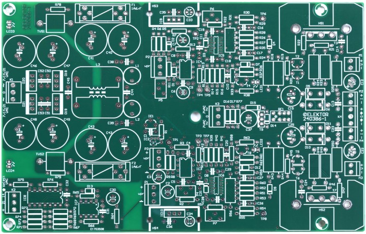
Fig. 13. PCB for the regulator (240386-1 v2.0).
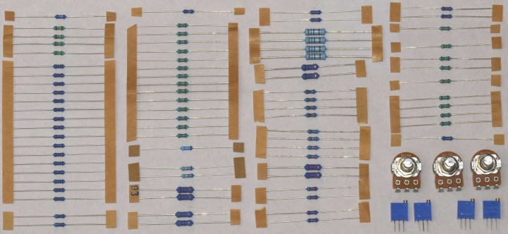
Fig. 14. Resistors and potentiometers for the regulator PCB (240386-1 v2.0).
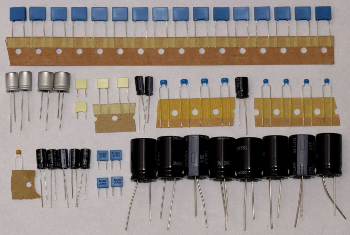
Fig. 15. Capacitors for the regulator PCB (240386-1 v2.0).
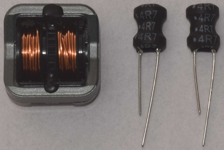
Fig. 16. Inductors for the regulator PCB (240386-1 v2.1).
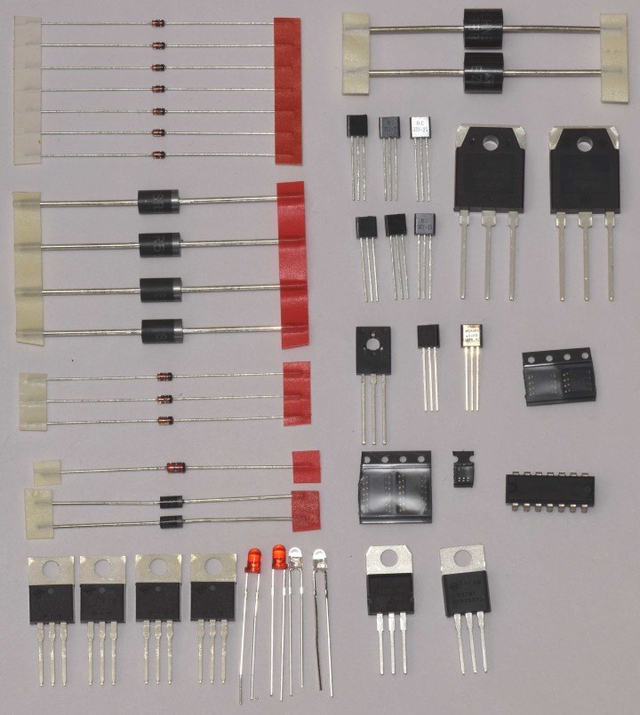
Fig. 17. Semiconductors for the regulator PCB (240386-1 v2.0).
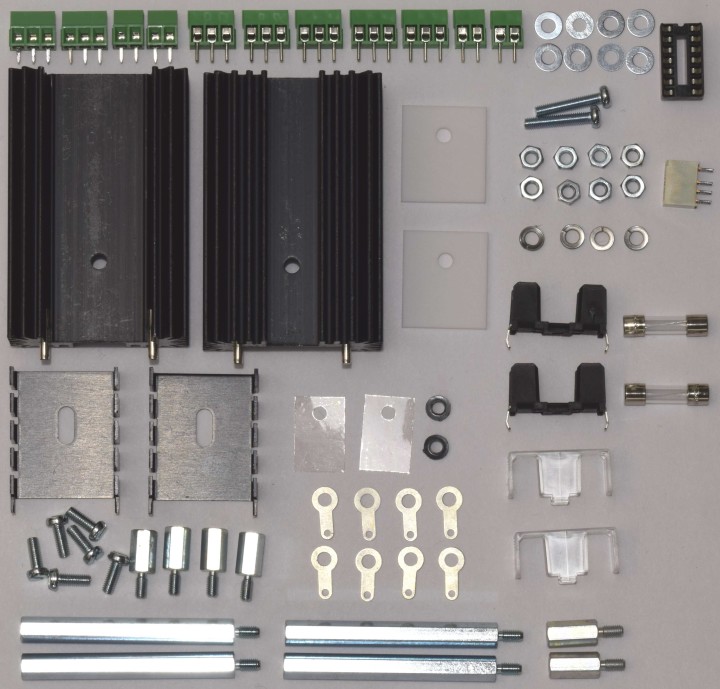
Fig. 18. Other parts for the regulator PCB (240386-1 v2.0).
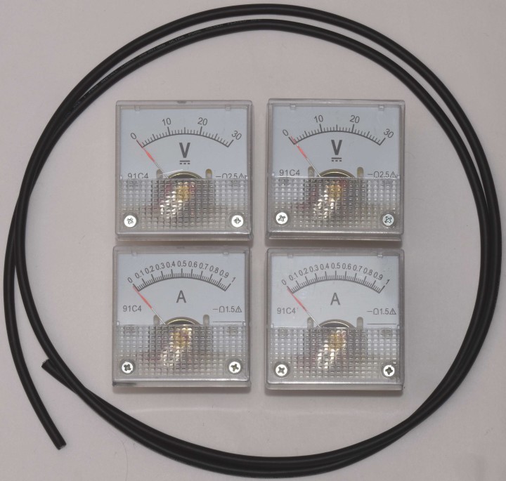
Fig. 19. Panel meters and 1-pair shielded cable to connect the potentiometers on the front of the enclosure.
Start with placing the lowest components first, from small diodes, resistors, power resistors to the heatsinks and the two power transistors in the output stage.
Recommended order:
Diodes D1, D2, D3, D4, D5, D9, D10, D11, D15
Diodes D8, D14, D16
Zener diode D17
Resistors R1, R2, R8, R37, R62, R3, R7, R10, R13, R17, R20, R22, R30, R33, R35, R42, R45, R47, R55, R58, R60, R4, R5, R6, R9, R12, R14, R16, R36, R38, R39, R41, R61, R63, R66, R72, R78, R79, R11, R15, R40, R21, R46, R26, R28, R51, R53, R27, R29, R52, R54, R32, R57, R34, R59, R64, R69, R65, R67, R80, R68, R70, R71, R73, R74, R75, R76, R77
SMDs IC5, IC6
Diodes D18, D19
Zener diode D24
1 W resistors R18, R43, R19, R44, R25, R50, R31, R56
1W resistors R23, R24, R48, R49 (depending on the exact type, if thicker mount the other 1 W resistors first)
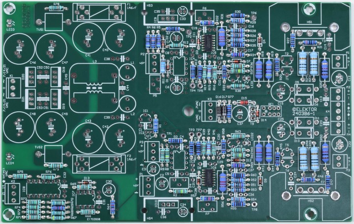
Fig. 20. Lowest components mounted, resistors, small diodes and IC5 and IC6 (PCB 240386-1 v2.0).
Ceramic capacitors C1, C50, C51, C52, C53, C35, C36, C44, C45
Diodes D6, D7, D12, D13
IC socket for IC8
PET capacitors C10, C20, C11, C21, C16, C26, C17, C27
Relay RE1
PET capacitors C4, C5, C8, C9, C13, C14, C18, C19, C23, C24, C28, C29, C31, C32, C38, C39
Screw terminal blocks K1, K2, K3, K4, M1, M2, M3, M4, P1, P2, P3 (slide M2 and M4 into K4 first)
Transient Voltage Suppressors TVS1, TVS2
Transistors T1, T2, T4, T5, T6, T8, IC1, IC2
2way pin headers for LED1, LED2, LED3, LED4
Trimmer potentiometers P4, P5, P6, P7
Fuse holders F1, F2
Inductors L1, L2
Electrolytic capacitors C12, C22, C15, C25
Electrolytic capacitors C2, C3, C6, C7, C30, C33, C34
Transistor T9
Electrolytic capacitor C37
Insert IC8 in socket
Diodes D20, D21, D22, D23
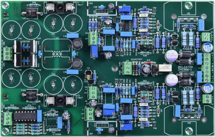 Fig. 21. Small capacitor, small transistors, diodes, screw terminal blocks and other low components mounted (PCB 240386-1 v2.0).
IC3, IC4, IC7 (all three SMDs on bottom side)
Common mode choke L3
Capacitors C40, C41, C42, C43, C46, C47, C48, C49
4 10 mm M3 standoffs (in mounting holes)
IC9, IC10, each mounted on heatsink HS3 and HS4 (FK222SA220) first:
Needed: 2 x heatsink SK222SA220A, 2 x 8 mm M3 screw, 2 x M3 nut, 2 x M3 washer, 2 x insulating bushing.
Apply a thin layer of heat transfer compound on one side of each mica insulation, that’s the side that’s placed against the heatsink. Also apply a thin layer of heat transfer compound on the back of IC9 and IC10 and place them against the mica insulation. Place the screw in the middle of slot of the heatsink. Place the head of both screws toward the edge of the PCB so they are still accessible with a screwdriver. Do not tighten the screw. Place each IC with the heatsink on the PCB. Make sure the heatsinks H3 and H4 are perpendicular to the PCB and then tighten the screw. Only then solder the three leads of the ICs.
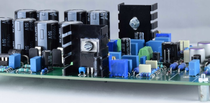
Fig. 22. Mounting of IC9 and IC10 on the small heatsinks (PCB 240386-1 v2.0).
Heatsink HS1 and HS2. Solder the two pins of each heat sink while making sure both are placed flat against the PCB. Make thermal reliefs in the leads of T3 and T7. Use special pliers like in the next photo or standard round nose pliers. The reliefs should be close enough to the package of the transistor so the mounting hole of the transistor and the heat sink will line up.
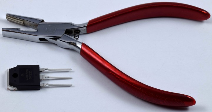
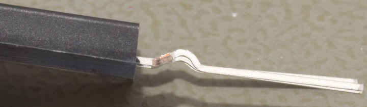
Fig. 23. Thermal reliefs in the leads of one of the power transistors. Also the special pliers used is shown.
Apply a thin layer of heat transfer compound on one side of each ceramic thermal pad. That side is placed against the heatsink. Also apply a thin layer of heat transfer compound on the back of T3 and T7 and place them against the ceramic thermal pads. Use the 16 mm M3 screw, M3 nut, M3 washer and M3 spring washer to mount T3 and T7 onto their heat sinks. Tighten the screws and solder the leads.
Place the fuses in the fuse holders and place the fuse holder covers.
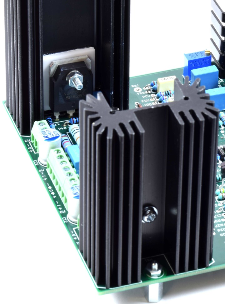
Fig. 24. Mounting of T3 and T7 on the heatsinks (PCB 240386-1 v2.0).
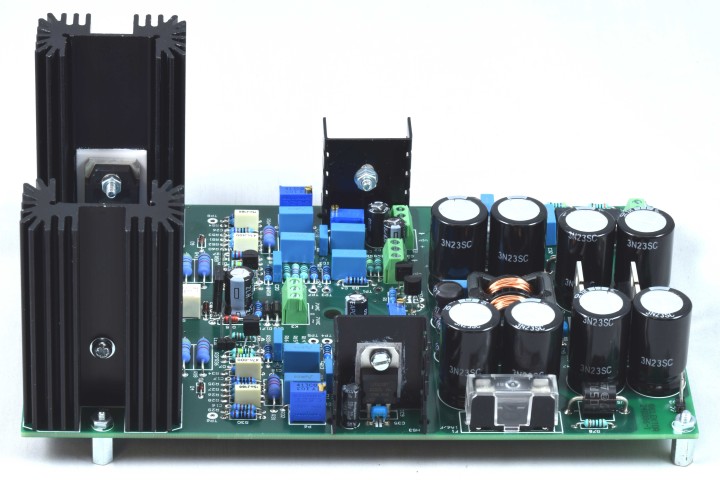
Fig. 25. Finished mounting components on the regulator PCB (240386-1 v2.0).
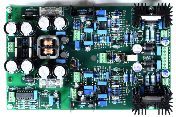
Fig. 26. Top view on the finished regulator PCB (240386-1 v2.0).
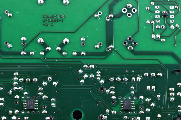
Fig. 27. Bottom view on the SMD ICs IC3, IC4 and IC7 (PCB 240386-1 v2.0).
Before placing everything inside an enclosure it’s better to test everything. When testing it’s probably easier to solder the 4 LEDS to the 2way pin sockets and place them on the pin headers on the PCB. Of course connecting the LEDs through thin stranded wire to the sockets is also an option since at least LED1 and LED2 are to be placed on the front of the enclosure.
Bill of Materials (PCB 240386-1 v2.1)
Resistor
R1 = 12 Ω, 250 mW, 1 %
R2, R8, R37, R62 = 1 MΩ, 250 mW, 1 %
R3, R7, R10, R13, R17, R20, R22, R30, R35, R42, R45, R47, R55, R60 = 100 Ω, 600 mW, 1%
R4, R5 = 4.7 kΩ, 250 mW, 1 %
R6 = 100 kΩ, 250 mW, 1 %
R9, R12, R14, R36, R38, R39, R61, R63, R66, R72, R78, R79 = 10.0 kΩ, 600 mW, 1 %
R11 = 9.76 kΩ, 600 mW, 1 %
R15, R40 = 44.2 kΩ, 600 mW, 1 %
R16, R41, R77 = 1 kΩ, 250 mW, 1 %
R18, R43 = 1.5 kΩ, 1 W, 5 %
R19, R44 = 470 Ω, 1 W, 5 %
R21, R46 = 330 Ω, 600 mW, 1 %
R23, R24, R48, R49 = 1.0 Ω, 1 W, 1 %
R25, R50 = 1 kΩ, 1 W, 5 %
R26, R28, R51, R53 = 1.000 kΩ, 250 mW, 0.1 %, 15 ppm/C
R27, R29, R52, R54 = 10.00 kΩ, 250 mW, 0.1 %, 15 ppm/C
R31, R56 = 1.2 kΩ, 1 W, 5 %
R32, R57 = 47 kΩ, 250 mW, 1 %
R33, R58 = 270 Ω, 250 mW, 1%
R34, R59 = 27 kΩ, 250 mW, 1 %
R64, R69 = 12.0 kΩ,, 250mW, 1 %
R65 = 3.0 kΩ, 600 mW, 1 %
R67, R80 = 470 Ω, 600 mW, 1 %
R68, R70 = 6.8 kΩ, 600 mW, 1 %
R71 = 30.0 kΩ,, 600 mW, 1 %
R73, R74, R75, R76 = 10 MΩ, 250 mW, 1 %
P1, P2, P3 = 10 kΩ, 200 mW, 20 %, potentiometer, 1 turns, single, lin., panel mount
P4, P5 = 500 Ω, 500 mW, 10 %, trimmer, 25 turns, 3296Y-1-501LF Bourns
P6, P7 = 10 kΩ, 500 mW, 10 %, trimmer, 25 turns, 3296Y-1-501LF Bourns
Capacitor
C1 = 100 nF, 50 V, 10 %, ceramic X7R, LS 5 mm
C2, C3, C6, C7, C30 = 10 uF, 63V, 20 %, LS 2.5 mm, 3000hours@105°C
C4, C5, C8, C9, C13, C14, C18, C19, C23, C24, C28, C29, C31, C32, C38, C39 = 100 nF, 250 V, 10 %, PET, LS 7.5 mm
C10, C20 = 47 nF, 100 V, 5 %, PET, LS 5 mm
C11, C21 = 10 nF, 100 V, 5 %, PET, LS 5 mm
C12, C22 = 220 uF, 35 V, 20 %, 0.024 Ω, LS2.5/3.5 mm, Ir 3.4 A, 2000hours@125°C, polymer
C15, C25 = 120 uF, 50 V, 20 %, ESR 0.02 Ω, Diam. 10 mm max., LS 5 mm
C16, C26 = 15 nF, 100 V, 5 %, PET, LS 5 mm
C17, C27 = 47 nF, 100 V, 5 %, PET, LS 5 mm
C33, C34 = 22 uF, 50 V, 20 %, LS 2 mm, 10000 hours @ 105°C
C35, C36, C44, C45 = 1 uF, 100 V, 10 %, LS 5 mm, ceramic X7R
C37 = 100 uF, 50 V, 20 %. LS 3.5 mm
C40, C41, C42, C43, C46, C47, C48, C49 = 1000 uF, 50 V, 20 %, LS 5/7.5 mm, Ir 3.32 A, 10000hours@105°C, D 16 mm
C50, C51, C52, C53 = 47 nF, 100 V, 10 %, ceramic X7R, LS 5 mm
Inductor
L1, L2 = 4.7 uH, 3.2 A, 0.033 Ω, LS 5 mm, RLB0914-4R7ML Bourns
L3 = Commom mode choke, 14.5 mH, 3 A, SSRH24NH-30145 Kemet
Semiconductor
D1, D2, D3, D4, D5, D9, D10, D11, D15 = BAT85, DO-34
D6, D7, D12, D13 = SR560, DO-201AD
D8, D14, D16 = 1N4148, DO-35
D17 = Zenerdiode, 5.6 V, 0.5 W, DO-41
D18, D19 = 1N4004, DO-41
D20, D21 D22, D23 = V30100CI-M3/P, dual commom cathode, TO-220
D24 = Zener diode, 30 V, 1 W, DO-41
LED1, LED2 = LED, red, T-1 (3 mm)
LED3, LED4 = LED, green, T-1 (3 mm)
TVS1, TVS2 = BZW50-33B, R6
T1, T2, T4 = BC337.25, TO-92
T3 = NJW0302G, TO-3P
T5, T6, T8 = BC327.25, TO-92
T7 = NJW0281G, TO-3P
T9 = BD139, TO-126 (SOT-32)
IC1 = LM334Z, TO-92+A69:DA69:I69
IC2 = LM4040AIZ-5.0/NOPB, TO-92 (TO-226AA-3)
IC3, IC4 = OPA2992IDR, SOIC-8
IC5, IC6 = OPA4992IDR, SOIC-14
IC7 = OPA992IDBVR, SOT-23-5
IC8 = LM339N, DIP-14
IC9 = LM317, TO-220
IC10 = LM337, TO-220
Other
K1, K4 = 3way screw terminal block, LS 3.5 mm, max. 1.5 mm²
K2, K3, P1, P2, P3 = 3way screw terminal block, LS 3.5 mm, max. 1 mm²
M1, M3 = 2way screw terminal block, LS 3.5 mm, max. 1 mm² (for M1/M3)
M2, M4 = 2way screw terminal block, LS 3.5 mm, max. 1.5 mm² (for M2/M4)
LED1, LED2, LED3, LED4 = Pin header, 1x2, vertical, pitch 2.54 mm
LED1, LED2, LED3, LED4 = Pin socket, 1x2, vertical. pitch 2.54 mm
HS1, HS2 = Heatsink MC33271 (for T3/T7), 2.7 °C/W, PCB mount, height 63.5 mm
IC9, IC10 = Heatsink FK222SA220, 20 °C/W, PCB mount
T3, T7 = Ceramic thermal pad (for T3/T7), 23 x 20 mm x 2 mm
IC9, IC10 = Insulating bushing IB 6, TO-220 (for IC9/IC10)
IC9, IC10 = Mica thermal pad for TO-220 (for IC9/IC10), 12 x 18 x 0.05 mm
M3 washer, plain, steel
M3 screw, 16 mm, steel, pan head
M3 nut
M3 spring washer
RE1 = Relay DPDT,5V, UA2-5NU
F1, F2 = PCB Fuse Holder, for 5 x 20 mm fuse, 10 A
F1, F2 = Cover for PCB Fuse Holder, transparent
F1, F2 = 5 x 20 mm fuse, 1.6 A, fast acting
M1, M3 = Moving coil meter, Range 30 V, type 91C4, 45 x 45 mm
M2, M4 = Moving coil meter, Range 1 A, type 91C4, 45 x 45 mm
M1, M2, M3, M4 = M3 solder lug, thickness 0.35 mm (to connect M1…M4)
M4 solder lug, thickness 0.35 mm (to connect 4 mm banana connectors)
to connect P1,P2,P3 = Screened cable, 1 pair, 2 x 24 AWG/0.22 mm², 1 m
IC8 = IC socket, DIP, 14 contacts
50 mm M3 standoff, steel, male-female
12 mm M3 standoff, steel, male-female
10 mm M3 standoff, steel, male-female
M3 screw, 8 mm, steel, pan head
Interested in a kit of parts for this project?
Back this project on its JumpStarter page!
About the PCBs
Mains filter PCB
Both top and bottom have a ground plane. Al pins of components connected to the mains voltage have a clearance of 3 mm. The power supply is a class I device, the metal enclosure must also be connected to mains-ground. One mounting hole of the PCB is connected to ground, the one next to K1. If the PCB is mounted with metal standoffs the connection of a metal enclosure to ground is ensured. Screw terminal K2, the output of the filter, also has a ground connection but is not used here.
Transformer PCB
The size of the transformer PCB is primarily determined by the three encapsulated toroidal PC transformers. Each transformer requires its own primary fuse. 3 jumpers must be placed to configure the 2 primary windings for 115 VAC or 230 VAC. For each transformer the layout of the jumper wire is such that two jumper wires for 115 VAC must be placed and only a single jumper wire for 230 VAC, but not all three can or should be placed!

Fig. 28. A single jumper wire per transformer for 230 VAC mains voltage.
The correct mains fuses must be used, the values are placed on the PCB: 3 x 160 mA/T in case of 230 VAC or 3 x 315 mA/T in case of 115 VAC.
Located on the secondary side of the transformers is the relay circuit to select the correct AC voltage and the POWER ON indicator LED1. The footprint of the LED is suitable for a standard 2way pin header (0.1” spacing). Screw terminals K2, K3 and K4 are positioned with short connections between the transformer PCB and regulator PCB in mind. To keep voltage drop from the transformers to the regulator PCB as low as possible all copper tracks of the secondary voltages to the relays and from the relays to K2 are wider than strictly needed. All secondary windings are easy accessible by several test points alongside the transformers:
7 VAC : TP1 and TP4, both TR2
14 VAC: TP2/TR1 and TP5/TR3
21 VAC: TP3/TR1 and TP6/TR3
GND: TP7
Because of the weight of the transformers the PCB has 8 mounting holes and make certain the PCB can be fitted securely inside an enclosure. A nineth mounting hole is located next to C1 so the regulator PCB can be mounted over the transformer PCB, if a higher than wide enclosure is preferred. However, this is not recommended. Due to the magnetic fields of the transformers it’s best to keep them at some distance from the regulator circuits.
Regulator PCB
The placement of all components follows the signal flow from the AC input voltage (K1) on one side to the regulated DC output voltages on the other side (K4) as best as possible. The ground connection from the smoothing capacitors C38…C43 to K4 is separated from all other ground connections. Ground planes on top and bottom of both regulator circuits connect all their ground connections to K4 only. Ground return currents from the external loads can only flow from K4 back to the smoothing capacitors, preventing offset voltages in ground connections. There’s a single bottom ground plane for the regulators, since several signals are cross connected between the two circuits and the ground potential must be the same and no large ground currents flow here. The larger heat sinks for the power transistors have two solderable pins connected to the ground planes. These transistors are insulated since the voltage of the collector, the metal tab of the package, is connected to the respective regulated output voltage. The smaller heat sinks of IC9 and IC10 are not grounded and have non solderable flat pins placed in non-plated PCB holes without pads. The relay circuit is positioned to keep the distance from each break contact close to its connection in the regulator. A hole in the PCB, also non-plated without pads, is placed next to K3 so wires connected to the 7 VAC voltage of the transformer PCB can be placed underneath the PCB to prevent these three wires lay on top of the circuit of the positive regulator. A standard 2way pin header (0.1” spacing) will also fit in the footprint of all 4 LEDs. The diodes of the rectifier (D20…D23) and the first set of smoothing capacitors (C45…C51) are placed close together. The ground connection to the output is placed underneath common mode choke L3. Next to the rectifier and the smoothing capacitors is sufficient room for the inverting amplifier IC7 and quad-comparator IC8. Tracks of +Vout and -Vout from K4 to IC7 and IC8 on the opposite side of the PCB, are placed along side the edge of the PCB. IC5 and IC6 have SO-14 packages and are placed on the top side. IC3 and IC4 have SO-8 packages and are placed on the bottom side. This way a SO-8 footprint can be combined without vias with a DIP-8 package on the top side. The pads of the DIP version make measuring easier. For the same reason is IC7 placed on the bottom side. The largest package of the OPA992 is a 5 pin SOT-23. This footprint is also combined with the pinning of a single opamp in a DIP-8 package. This way its easy to measure pins of IC7 from the top side. Of the PCB. Despite the very small size the SOT-23 is still solderable with a soldering iron with a fine tip and thin solder.
Adjusting the 4 trimmers
A few power resistors as loads are needed or an adjustable electronic load or something similar.
Trimmer P4 is added in case of an unlikely condition where the maximum output current, from one or both regulators, is less than 1 A. It sets the level of +Iset (TP3). The maximum output current(s) can be increased a little, by 50 mA (P4/R9 = 500/10000 A). If this is not enough check all components. Connect a load through which the output is slightly overloaded and the output voltage goes down. For instance set the output voltage to 22 V and connect 20 Ω (like two 10 Ω / 10 W resistors). The output voltage should go down to 20 V, probably a little higher because of series resistances in the connection to the load and multimeter.
P5 is the adjust for -Iset and can be set two ways. The best is to measure the maximum output current of the negative regulator and set it to 1 A or a little bit higher. Use the same procedure as described for P4. An other way is to simply make the level of-Iset (TP4) the exact inverted of +Iset (TP3).
P6 and P7 can each be set two ways. Set current control P3 to minimum ( 0 A) and adjust P6 and P7 so the output currents are minimal, they should be less than 10 mA. Another way is to look at the output voltages without a load. In case the minimum current is set with P6 and P7 the out voltages will go down when P3 is set to 0 A, even without loads, but not fully to 0 V. Because of tolerances these voltage are different for the positive and negative regulator. Turning P6 and P7 completely the opposite way the output voltages will increase. Experiment with loads with higher impedances to see which setting is the preferred one.
Interested in a kit of parts for this project?
Back this project on its JumpStarter page!
Specifications
Output voltage 0…+22 V, 0, -22 V
Output current 0…+1 A, 0…-1 A
Noise -85 dBV, (at 0.95 A / 20 V, B = 22 kHz)
Noise -84 dBV (at 0.95 A / 20 V, B > 500 kHz)
Ripple 50 uVRMS (at 950 mA / 20 V, B = 22 kHz, mainly 100 Hz component)
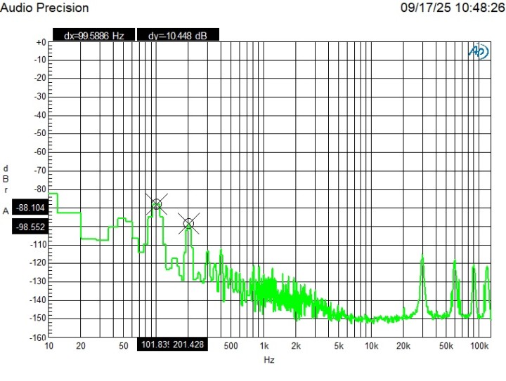
Fig. 29. Spectrum at 20 V and 0.95 A. 30 kHz component and its harmonics are environmental, not from the PSU.
A quick check:
Test points are added to the PCB to make measuring with a probe a little easier:
TP1 is -Vset, IC3B: 0…+5 V
TP2 is +Vset, IC4A: 0…-5 V
TP3 is +Iset, IC3A: 0…+5 V
TP4 is -Iset, IC4B: 0…-5 V
TP5 is output IC5B: output voltage plus approximately 0.6 to 1.4 V, depending on load
TP6 is output IC5D: 0 to +5 V, depending on output current
TP7 is output IC6C: output voltage minus approximately 0.6 to 1.4 V, depending on load
TP8 is output IC6A: 0 to -5 V, depending on output current
At 1 A about 82 mV is lost across 1.6 A fuses F1 and F2.
At 1 A the ripple voltage at the input of the regulator stages is less then 1.6 Vpp
A self-made enclosure, just as an example
No standard enclosure was chosen for this power supply, they’re either too small or too big, have wrong dimensions or are too expensive and don’t have enough holes or slots for sufficient ventilation. Instead a custom version was made from aluminum plates and aluminum angles (to join the plates). This example is just a rectangular “box”, but it’s a solid one. Use your own imagination to create something better looking. The aluminum angles are equilateral, 15 x 15 mm and 3 mm thick. The top plate and the two sides are perforated to ensure sufficient airflow. Aluminum plates can be ordered in various shops and have them cut to size.
Dimensions of the plates and angles:
Plates:
Front and back 2 x 300 x 90 mm, 2 mm thick
Bottom 1 x 300 x 250 mm, 3 mm thick
Top 1 x 300 x 250 mm, 2 mm thick, 35 % perforated, holes 5 mm, distance 8 mm
Sides 2 x 250 x 85 mm, 2 mm thick, 35 % perforated, holes 5 mm, distance 8 mm
Angles, 15 x 15 mm, 3 mm thick:
Front and Back 4 x 296 mm
Sides 4 x 220 mm
Corners 4 x 55 mm
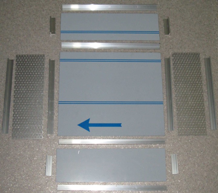
Fig.30. All plates and angles except top plate.
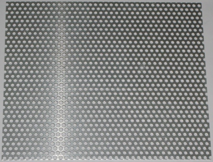
Fig. 31. The perforated aluminum top plate.
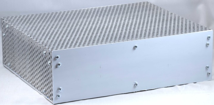
Fig. 32. The enclosure made of the 6 aluminum plates and angels. Protective adhesive foils not removed yet.
Next to do is drilling holes for the standoffs and screws, banana connectors, potentiometers and the LEDs. Also create larger holes for the moving coil meters and the IEC mains power inlet with switch in the back.
Wiring
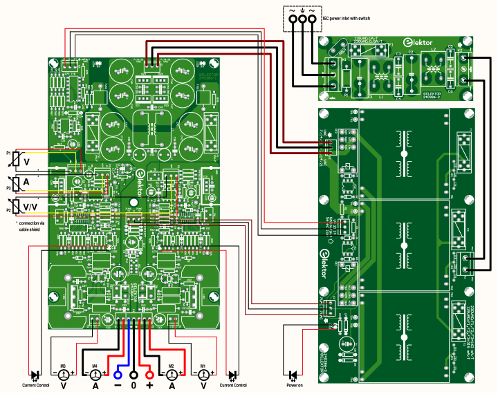
Fig.33. Wiring diagram.
Wires used for connections between PCBs, to output sockets, panel meters, potentiometers and IEC power inlet:
IEC C14 power entry module to K1 mains filter PCB: 0.75 mm2, 3 core, unscreened (3183Y-0.75MMWHT Multicomp Pro)
K2 mains filter PCB to K1 transformer PCB: 0.75 mm2, 3 core, unscreened (3183Y-0.75MMWHT Multicomp Pro)
K2 transformer PCB to K1 regulator PCB: 1.5 mm2 (transformer output voltages)
K3 transformer PCB to K3 regulator PCB: 0.25 mm2 (to detect presence mains voltage)
K4 transformer PCB to K2 regulator PCB: 0.25 mm2 (signals to set transformer voltage)
Voltage outputs: 1.5 mm2 (connect the output K4 regulator PCB to 4 mm banana connectors on the front of the enclosure)
M2, M4 regulator PCB to moving coil amperemeters on front: 1.5 mm2
M1, M3 regulator PCB to moving coil voltmeters on front: 0.25 mm2
Potentiometers connected by high quality screened cable, 1 pair, 2 x 24 AWG/0.22 mm² (Multipair Cable 268001CL Van Damme). A total of 75 cm should be enough for three pieces of screened cable.
Additional components needed:
3 banana connectors (Hirschmann PKI110 series red, black and blue)
An un-filtered IEC power entry module (no fuse) for the mains voltage (Schurter DC11.0001.003)
3 knobs, round shaft 6.35 mm, aluminum, 14 mm round with indicator line (Multicomp 14S-2D)
M3 screws and nuts
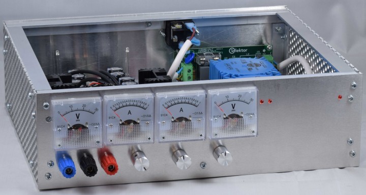
Fig. 34. Finished prototype. Everything is wired.
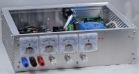
This picture above and the next two give a good impression of what the power supply can look like and orientation and placement of the PCBs and all other parts.
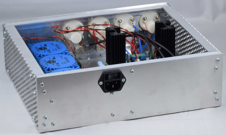
Fig. 35. View on the back. Only the IEC power inlet with integrated mains switch is placed here.
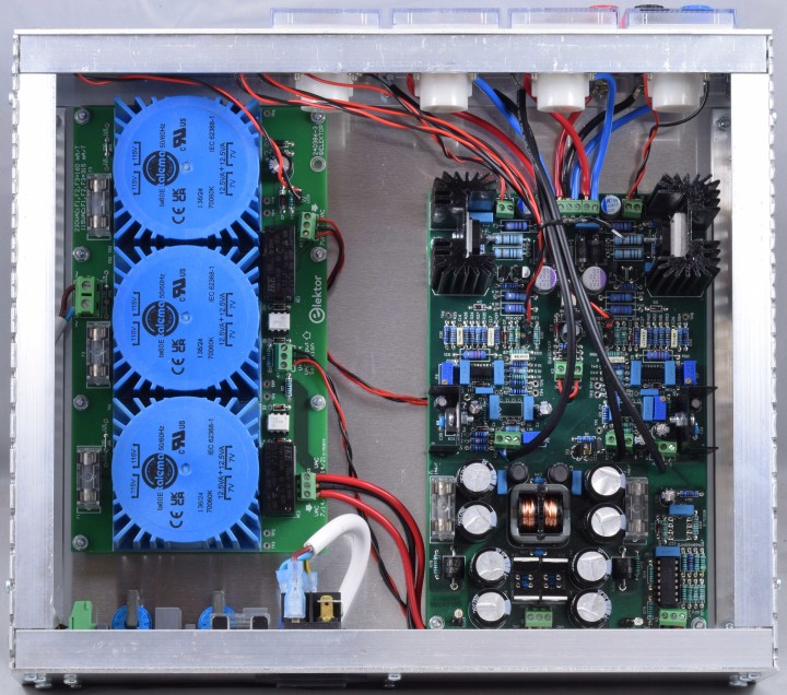
Fig. 36. Top view on the finished power supply.
Use heat shrink tubing to cover the solder joints of soldered wires where possible. If you look closely you can see a bare terminal of the mains switch in the bottom of the picture. Although the creepage distance is more than enough, even with the top panel in place, additional insulation is recommended since the top panel is perforated!
What’s missing is an extra 4 mm banana connector connected to the metal enclosure for grounding.
Alternate positioning Regulator and Transformers
It is possible to create a more compact assembly of the power supply by placing the regulator PCB on top of the transformers. The transformer PCB has a ninth mounting hole (right next to C1), this way two mounting holes have the same distance as two on the regulator PCB. The mounting hole in the corner next to it can be left unused. This side of the regulator PCB is fastened with 2 50 mm standoffs on top of the transformer PCB and so two 10 mm standoffs of the regulator are not needed. Two 50 mm and two 12 mm standoffs are used to fasten the other side of the regulator PCB directly to the bottom of the enclosure (just alongside the transformer PCB). The following 5 photo’s show this alternate assembly. However, close proximity of the transformers to the regulator PCB is not advised, the magnetic fields of the transformers can interfere with the regulator circuits and degrade performance. This configuration is not tested and will likely compromise the working and specifications of the regulator.
Interested in a kit of parts for this project?
Back this project on its JumpStarter page!
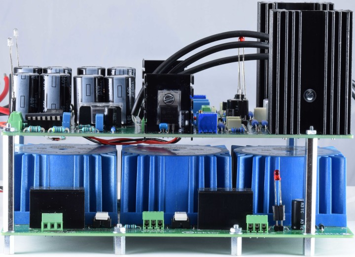
Fig. 37. Alternate assembly of the regulator PCB and transformer PCB.
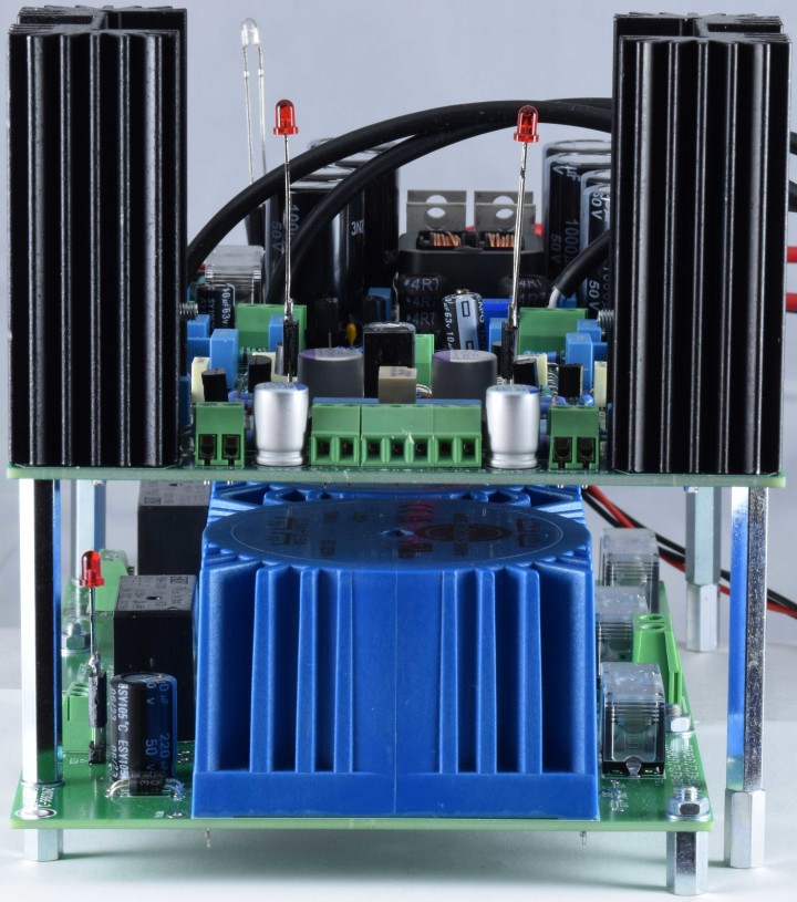
Fig. 38. Alternate assembly of the regulator PCB and transformer PCB.
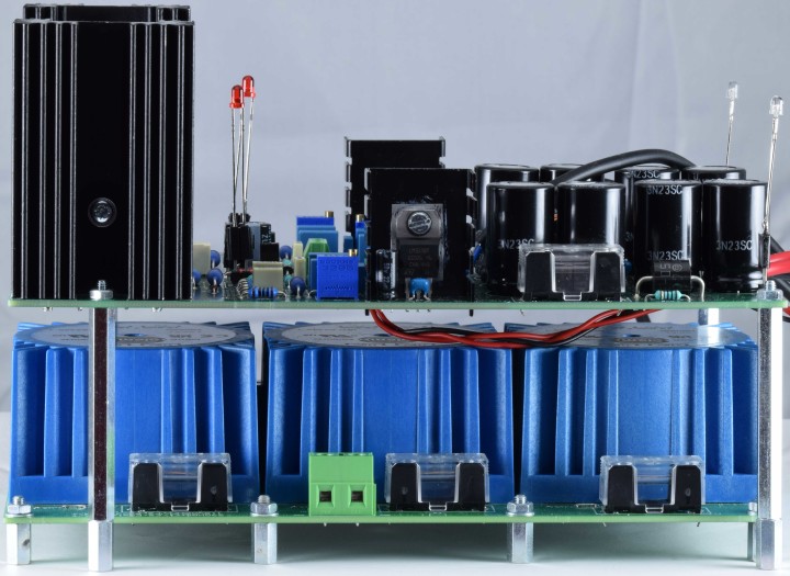
Fig. 39. Alternate assembly of the regulator PCB and transformer PCB.
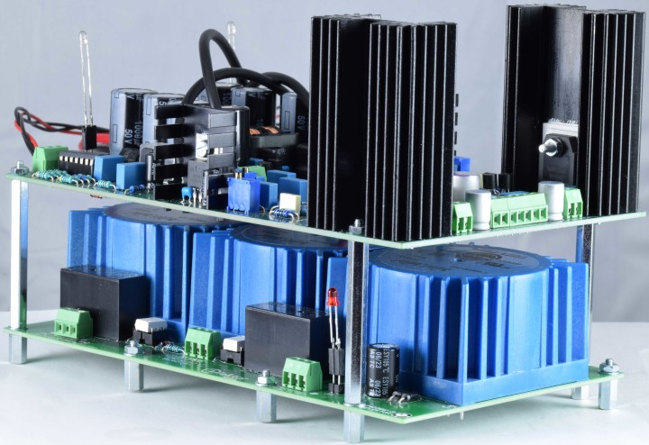
Fig. 40. Alternate assembly of the regulator PCB and transformer PCB.
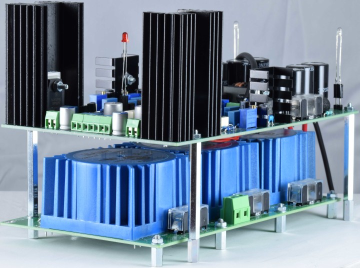
Fig. 41. Alternate assembly of the regulator PCB and transformer PCB.
Web links
https://www.hagtech.com/pdf/snubber.pdf
https://sound-au.com/articles/cmpd-vs-darl.htm
PCB layouts
Regulator
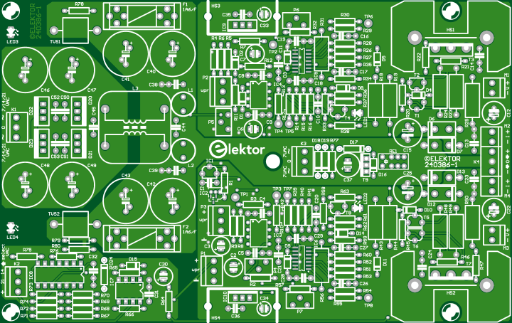
Fig. 42. Top overlay of the PCB of the Low Noise Power Supply Unit 240386-1 v2.1.
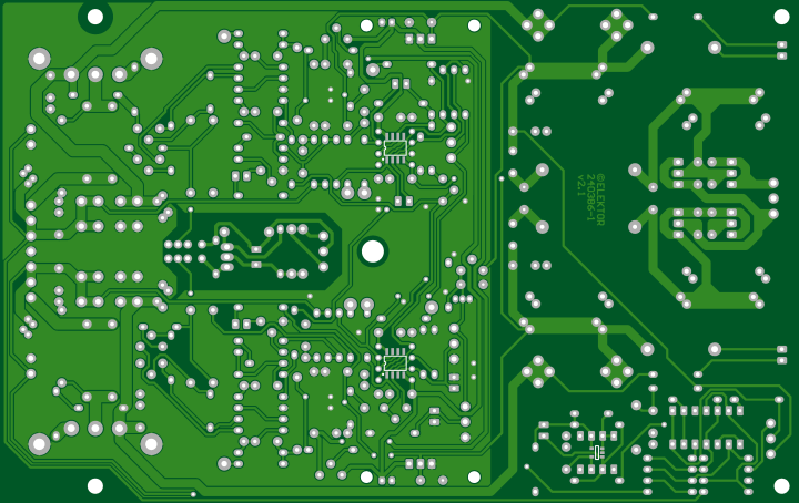
Fig. 43. Bottom overlay of the PCB of the Low Noise Power Supply Unit 240386-1 v2.1.
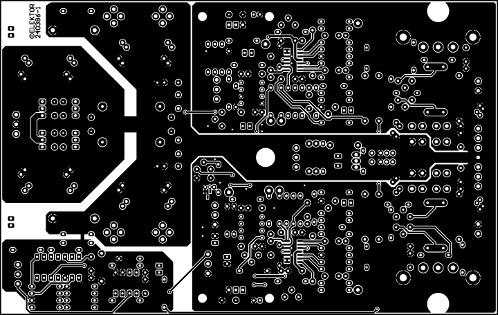
Fig. 44. Copper on top of the PCB of the Low Noise Power Supply Unit 240386-1 v2.1.
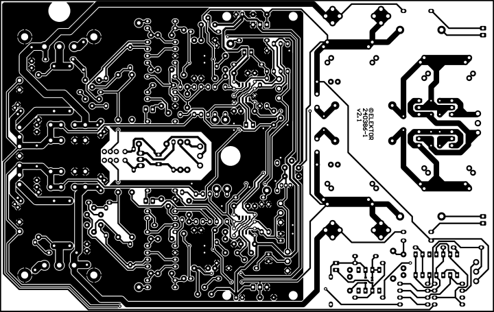
Fig.45. Copper on bottom of the PCB of the Low Noise Power Supply Unit 240386-1 v2.1.
Mains filter
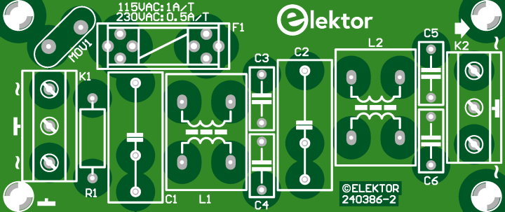
Fig. 46. Top overlay of the PCB for the Low Noise Power Supply Unit 240386-1 v2.1.

Fig. 47. Bottom overlay of the PCB for the Low Noise Power Supply Unit 240386-2 v2.1.

Fig. 48. Copper on top of the PCB for the Low Noise Power Supply Unit 240386-2 v2.1.

Fig.49. Copper on bottom of the PCB for the Low Noise Power Supply Unit 240386-2 v2.1
Transformers
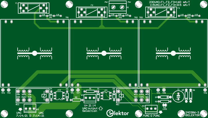
Fig. 50. Top overlay of the transformer PCB for the Low Noise Power Supply Unit 240386-3 v2.0.
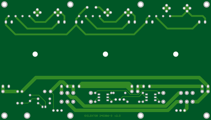
Fig. 51. Bottom overlay of the transformer PCB for the Low Noise Power Supply Unit 240386-3 v2.0.
Fig. 52. Copper on top of the transformer PCB for the Low Noise Power Supply Unit 240386-3 v2.0.
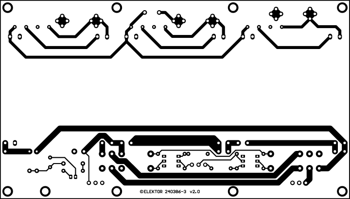
Fig. 53. Copper on bottom of the transformer PCB for the Low Noise Power Supply Unit 240386-3 v2.0.
Interested in a kit of parts for this project?Most laboratory power supplies and AC adapters these days are switched mode types. Even the best of them still have a high frequency ripple and other artifacts present on the output voltage, inherent to their design. When testing sensitive analog circuits this can cause problems, interfere with low level measurements. So, why not design a fully analog power supply. Of course efficiency is less, but for testing purposes this is not an issue and ensures results are more reliable.
Since many analog circuits require a symmetrical supply voltage, this power supply has to have a symmetrical output voltage. The positive and negative output voltage have equal levels, with a limited adjustment to compensate any imbalance. Of course a variable current limit is also a requirement.
The first idea was to place both power transistors of the output stages on a common heat sink and use a single mains transformer with two equal secondary windings. However, design requirements are an adjustable output voltage of 0 to +/- 22 V and an adjustable current limit of 0 to +/- 1 A. In this setup a standard mains transformer with 2 x 22 V secondary voltages would be a good candidate to provide the source voltage for the regulator stages. However at a (permanent) short circuit condition with both outputs set to maximum current almost 60 W must be dissipated. To limit the temperature rise to 30 °C the thermal resistance of the heat sink must be approximately 0.5 °C/W. That’s a large heatsink. To limit the size of the heatsink to a minimum the input voltage of the regulators would have to be proportional to the output voltage. Taking in to account voltage drop across the rectifiers and inductors of the filters and fuse, ripple voltage across the smoothing capacitors and drop-out voltage of the regulator the input voltage would have be at least 3,5 V higher than the output voltage. Only a switched mode circuit or something similar could resolve this and of course no option here. Less perfect but still a good alternative is to use more than one secondary voltage and select a higher AC voltage in discrete steps when needed. Two AC voltages is a minimum but three is better and will reduce the size of the heat sink considerably. Even more so by using two heat sinks, one per output stage. The heat sinks are now small PCB mounted versions and as an additional advantage make the construction a lot easier. In a worst case scenario at 30 V input voltage and 1 A short circuit current, the power of 30 W would cause a temperature rise of 81 °C in the 2.7 °C/W heat sinks. The junction of the power transistor would still be lower than its specified maximum of 150 °C. But consider this, when the junction of a transistor is hotter than 70 °C for a prolonged time, this will reduce its lifespan. To protect against such an excessive temperature rise a thermal switch could be considered, not used here. Types exist that can switch mains voltages.
Instead of a single custom transformer with 6 secondary windings three identical transformers are used. The toroidal transformers are encapsulated PCB mounted versions and a separate PCB is designed (240386-3). This also makes the construction easier, the relay circuit to select the correct AC voltage is placed on this PCB and it can be mounted at some distance from the regulator PCB.
Noise from the mains voltage is reduced by a separate common mode filter with two common mode chokes, a smaller third PCB (240386-2).
To keep the design completely analog instead of digital panel meters 4 small moving coil meters indicate both output voltage and current of each regulator. Advantage of the moving coil meters is they don’t need an additional power supply. Accuracy and resolution is perhaps a bit lacking. But good practice is to use a multimeter to check the output voltage and current of any power supply. The connection of the current meter is placed inside the feedback loop of the output stage. This way its resistance has no influence on the output voltage.
Two window comparators (quad comparator IC8) select the AC input voltage needed for the regulators, one per output voltage. In case one of the current limits is active the highest output voltage determines the AC volage. Downside of this choice is the heat sink of the limiting output will get hotter because of the higher voltage drop across the power transistor. This is a choice to reduce the size of the regulator, not making it too complex.. Otherwise two AC inputs and rectifiers would be needed and would make the power supply more like two separate ones.
Higher efficiency could be achieved by using Ideal Diode Bridge Controller LT4320 for the rectifier. But it doesn’t work with a center tap transformer design to create symmetrical DC voltages. Two ICs would be needed with each 4 MOSFETs. That’s a bit extreme. So, to ensure a low as possible voltage drop a standard diode bridge with Schottky rectifiers is used. The V30100CI-M3/P contains two diodes in a TO-220 package, these are connected in parallel to lower the voltage drop across the rectifiers a little more.
Initially rail-to-rail-in-out opamps are used so only a single supply voltage per regulator is required, making the PCB design less complex. While testing an earlier concept a LT1677CN8 was used in a non inverting setup for the regulators. Depending on voltage rise of the supply voltages and input levels during this time the output of the opamp was locked to a low level, although input levels were well within its specifications when the power supply was settled. Extra input protection diodes solved it, the internal input protection diodes apparently are not preventing this problem. It has a very high absolute maximum supply voltage of 44 V and overall very good specifications. Ideal since it is directly connected to the rectified AC voltage. But its input bias current and limited differential input voltage, use as a true comparator is not possible, made it necessary to look for an alternative. The current control of the regulators uses one of the amplifiers as a comparator. The OPAx992 family was chosen. The maximum differential input voltage range is the supply voltage and input bias current is only ±1- pA. Also offset voltage, offset voltage drift and input noise are extremely low. Downside of newly developed opamps is the availability in SMD packages only. The PCB uses dual footprints for the single and dual versions of the opamps. This makes measurements easier and safer. The pads of the DIP footprint make it less likely a short circuits occurs by slipping of a probe. Sadly this is not possible with the quad version in any easy way. When measuring the pins of the quad versions be careful and measure a connected component instead of the lead of the IC itself.
Output current of each regulator is measured across a shunt in the output of the regulator. If the power supply was a single version the shunt could be placed in the ground terminal. But since there is a common ground here this is not possible. A differential amplifier is required to subtract the common mode voltage, which is in fact the output voltage. To increase the precision of the measured voltage across the shunt the tolerance of the 4 resistors needs to be 0.1 %.
Depending on the level of the common mode input voltage of rail-to rail opamps specifications can vary. Often there’s a small range where the complementary differential input pairs are both active and some specifications are different. This region is close to one a the supply rails. To avoid this the regulators were changed to an inverting topology. This ensures both inputs of the opamps controlling the output voltage are always at ground level.
Interested in a kit of parts for this project?
Back this project on its JumpStarter page!
A positive refence voltage is created directly from the filtered and rectified AC voltage. To ensure a clean reference voltage a Precision Micropower Shunt Voltage Reference LM4040 is used. Its operating current is provided by Adjustable Current Source LM334 and is approximately 4.6 mA. 1 mA is flowing into P1 and P3. The combination of a current source and voltage reference suppresses any noise and interferences coming from the unregulated source voltage. The level of this rectified AC voltage depends on the output voltage of the regulators. The current source also keeps the operating current of the LM4040 independent of the input voltage. Both reference and current source are still available in a TO-92 package. The reference is also available in a SOT-23 package. The footprint combines both packages. This way also a newer LM4050 can be used, but the latter has a higher wide band noise than the LM4040, 93 µV instead of 80 µV (10 Hz to 10 kHz at 100 µA). This positive reference voltage is connected to the potentiometer (P1) that controls the level of both output voltages. Its wiper is buffered to create the positive control voltage -Vset for the negative regulator. An extra inverter is used to create the negative control voltage +Vset for the positive regulator. The gain of this amplifier is slightly adjustable (P2) to compensate for any difference in absolute voltage levels of the regulators. Current limit setting is the same for both regulators but independent of each other. Three single potentiometers are necessary and either single turn of multiturn potentiometers can be used, the latter being more expensive of course.
As said before, the intention to use rail-to-rail opamps was a simpler design. But several reasons made it necessary to use additional supply voltages, a low negative supply voltage for the positive regulator circuit and a low positive supply voltage for the negative regulator circuit. To create these two supply voltages a LM317 and LM337 were added. Connecting their adjust to ground creates +1.25 V and – 1.25 V. Rail-to rail sounds nice but in practice the output voltages are never equal to the supply rails. The residual voltage are the cause setting the current limit to 0 A was not 0. Two extra trimmers were added to compensate this partially. The two additional regulated supply voltages are also the reference voltages for these trimmers.
To filter any residual interferences from the transformer PCB a common mode filter and differential mode filters are added to filter the rectified voltages.
To prevent output voltages rise above the set values when the power supply is shut down a relay short circuits the drive of both output stages. The relay is powered by an isolated rectifier, connected separately to the transformer PCB, and a small smoothing capacitor to deactivate the relay instantly when the power supply is turned off. The relay also speeds ups the discharging of the (additional) capacitors connected to the outputs of the regulators through R19 and R44.
Mains filter
Mains voltages contain all kinds of noise and interferences. To use the mains voltage as a source for a low noise power supply it first has to be filtered. In most cases common mode interference is worse than differential mode interference, latter can often be filtered by a simple low pass RC filter or better yet an LC filter. To increase the suppression of these common mode signals instead of a single common mode choke two are used.
Fig. 1. Mains filter for the Low Noise Power Supply (240386-2 v2.1).
The schematic is standard. The capacitors C3…C6, connected from the mains voltage to ground are of type Y. The capacitors C1 and C2, connected between the mains voltage, are type X. The fuse is rated 500 mA when a mains voltage of 230 VAC is used, and 1 A in case of 115 VAC. The value depends on three times the primary fuse rating of the three mains transformers of the Low Noise PSU. Metal Oxide Varistor MOV1 protects against large voltage spikes. For 115VAC the S14K300 (ordering code B72214S0301K101) should be replaced by type S14K150 (ordering code B72214S0151K101). Resistor R1 discharges the capacitors when the filter is disconnected from the mains, should no load be connected to K2. K2 must be connected to K1 on transformer PCB 240386-3.
Construction mains filter PCB (240386-2 v2.0)
Fig. 2. PCB for the mains filter (240386-2 v2.0).
Fig. 3. All parts for the mains filter PCB (240386-2 v2.1).
Start by soldering de lowest components. Resistor R1 first and the common mode chokes L1 and L2 last.
Proposed order:
Resistor R1
Capacitors C3, C4, C5, C6
Fuse holder F1
Varistor MOV1
Capacitors C1, C2
Screw terminal blocks K1, K2
Common mode chokes L1, L2
Insert the fuse (500 mA T for 230 VAC or 1 A T for 115 VAC)
Place the cover for the fuse holder
Mounting of 4 standoffs can wait until an enclosure is constructed/adapted
The mains filter is now ready for use
Fig. 4. All parts fully mounted and soldered and the filter is ready for use.
Bill of materials PCB 240386-2 v2.1
Resistor
R1 = 220 kΩ, 1 W, 500V, 5 %
Capacitor
C1, C2 = 470 nF, 305 VAC, Class X2, 11x27 mm max., LS 15/22.5 mm
C3, C4, C5, C6 = 2.2 nF, 300VAC, Class Y2, 13x4 mm, LS 10 mm, PP
Inductor
L1, L2 = Common mode choke, 6.8 mH, 1.7 A, TDK B82732R2172B030
Semiconductor
MOV1 = TVS varistor, 300VAC S14K300
Other
K1, K2 = 3way screw terminal block, LS 7.62 mm
F1 = 0.5 A time delay, 250V, cartridge fuse 5 x 20 mm
F1 = 1 A time-lag, 250V, cartridge fuse 5 x 20 mm
F1 = Fuse holder 5x20 mm, 10 A, 500 VAC
F1 = Cover for fuse holder, transparent
4 x10 mm M3 standoff, steel, male-female
4 x M3 screw, 8 mm, steel, pan head
4 x M3 nut
Interested in a kit of parts for this project?
Back this project on its JumpStarter page!
Transformers
To keep the heat sink of each output stage of the two voltage regulators as small as possible, so types that can be mounted on the PCB can be used, the AC input voltage of the regulator is divided in three levels. This also improves overall efficiency. Two relays are controlled by the regulator to select the correct AC voltage, depending on the DC output voltage. Two optocouplers make sure there’s no ground loop between the AC input voltage of the regulators and the power ground of the relay coils. The MOC8021M has a very high current transfer ratio, minimum 1000 %.
Fig.5. Circuit with the 3 transformers for the Low Noise PSU.
The transformer chosen for the regulator has two separate symmetrical secondary windings. The two secondary windings of TR2 are connected and this is the GND connection of the outputs (K2 and K3). The two secondary windings of TR2 and TR3 are also connected and each transformer is connected to one of the secondary windings of TR1. This way 2x 7, 14 and 21 VAC with counterphase are available on K2. If RE1 and RE2 are turned off 2 x 7 VAC is selected. 2 x 14 VAC is selected if RE1 is turned on and RE2 is still turned off. If RE2 is turned on the output is 2 x 21 VAC independent of RE1. K3 is added to detect turning off the PSU or the sudden absence of the AC voltage on K2 to get the output of the PSU to 0 V as fast as possible. To power the relays the 2 x 21 VAC is rectified by D5, D6 and C1. D7 lowers this voltage to approximately 24 V, the nominal coil voltage of both relays. This voltage varies with current demand of the regulators. D3 and D4 limit the induction spike when the relays are turned off to protect the optocouplers. D1 and D2 prevent potential damage to the LEDs of the optocouplers caused by wrong polarity, for instance in case of faulty wiring.
The chosen transformer also has two separate symmetrical primary windings. These should be connected in series for 230 VAC mains voltage and in parallel for 115 VAC. The primary windings of each transformer are connected to 4 solder pads forming a jumper. 1 jumper wire must be placed for 230 VAC and 2 different jumper wires for 115 VAC.
LED1 can serve as a general POWER ON indicator on the front of the enclosure.
Construction transformer PCB (240386-3 v2.0)
Fig. 6. PCB for the 3 transformers and the surrounding components (240386-3 v2.0).
Fig. 7. All Parts for the transformer PCB (240386-1 v2.0).
Start by soldering de lowest components. Jumper wires first and transformers last.
Proposed order:
Jumper wires JP1, JP2 and JP3: 1 for 230 VAC per transformer, 2 for 115 VAC per transformer
Resistors R1,R2 and R3
Diodes D1, D2, D3 and D4
Diodes D5 and D6
Diode D7
DIP-6 IC sockets for optocouplers IC1 and IC2
Screw terminal blocks K2, K3 and K4 (K2 is the different one!)
Pin header for LED1
Fuse holders F1, F2 and F3
Insert the fuses (3 x 160 mA T for 230 VAC or 3 x 315 mA T for 115 VAC)
Place the covers for the fuse holders
Screw terminal block K1
Capacitor C1
Relays RE1 and RE2
Place the three transformers and fasten each with a 8 mm M4 screw and plane washer, only then solder the pins. Be careful when turning the screws inside the thread of the transformers, avoid applying excessive force! This could damage the M4 thread inside the transformers.
Insert optocouplers IC1 and IC2
Optional: LED1 can directly be soldered to the PCB or connected by thin stranded wire and a 2way pin header and socket, since it’s meant to serve as the power indication on the front of the enclosure.
Mounting of the 8 standoffs can wait until an enclosure is adapted/constructed
The transformer PCB is now ready for use.
Fig 8. All parts fully mounted and soldered and ready for use.
Fig. 9. Detailed view. Before soldering each transformer is fastened first to the PCB by a 8 mm long M4 screw.
Two side view photos:
Fig. 10. All parts mounted and soldered. Side view on the low voltage side.
Fig.11. All parts mounted and soldered. Side view on the mains voltage side.
Regarding the transformer PCB:
The transformer PCB is necessary to keep the power loss as low as possible. Design requirements are a symmetrical adjustable output voltage of 0 to 2 x 22 VDC with a common ground and an adjustable output current from 0 to 1 ADC (current limit). If a standard AC voltage of 2 x 22 VAC were to be used, at very low output voltages or sustained short circuit at both outputs and maximum output current, the maximum power loss would be around 60 W. A very large (common) heatsink would be needed and make it an inefficient design. Of coarse this in inherent to an analog PSU. But, by dividing the input voltage of the regulator in 3 levels, these depend on the output voltage, the power loss can be significantly reduced. A separate heatsink for each regulator instead of a very large common one makes the required heatsinks even smaller. Using three separate standard transformers prevents having to use a custom designed transformer with 6 secondary windings.
The PCB can be used with 230 VAC (50 Hz) and 115 VAC (60 Hz) mains voltages. Each transformer has two equal primary windings. For use with 230 VAC these must connected in series. This requires one jumper wire at position 230 next to each transformer. To use the transformer with 115 V AC the two primary windings must be connected in parallel. This requires two jumper wires at positions 115 next to each transformer. Each transformer is protected by a primary fuse of type time delay (also called slow acting), 160 mA for 230 VAC and 315 mA slow acting for 115 VAC.
Bill of materials PCB 240386-3 v2.0
Resistor
R1, R2 = 2.7 kΩ, 600 mW, 1 %
R3 = 10.0 kΩ, 600 mW, 1 %
Capacitor
C1 = 220 uF, 50 V, 20 %, D 10 mm, LS 5 mm, 4000 hours @ 105C
Transformer
TR1, TR2, TR3 = 2x 7 V, 25 VA, PCB mounted toroid, 70060K Talema
Semiconductor
D1, D2, D3, D4 = 1N4148, DO-35
D5, D6 = 1N4004, DO-41
D7 = Zener 5.6 V, 1.3 W, DO-41
LED1 = LED, red, T-1 (3 mm)
IC1, IC2 = MOC8021M, CTR 1000 % min., DIP-6
Other
K1 = 2way screw terminal block, LS 7.62 mm
K2 = 3way screw terminal block, LS 3.5 mm, max. 1.5 mm²
K3, K4 = 3way screw terminal block, LS 3.5 mm, max. 1 mm²
LED1 = Pin header, 1x2, vertical, pitch 2.54 mm
LED1 = Pin socket, 1x2, vertical. pitch 2.54 mm
F1, F2, F3 = Fuse holder 5x20 mm, 10 A, 500 VAC
F1, F2, F3 = Cover for fuse holder, transparent
F1, F2, F3 = 160 mA, time delay, cartridge fuse 5x20 mm
F1, F2, F3 = 315 mA, time delay, cartridge fuse 5x20 mm
RE1, RE2 = Relay DPDT, 5 A/250 VAC/24 VDC,
TR1, TR2, TR3 = M4 screw, 8 mm, pan head
TR1, TR2, TR3 = M4 washer, plain, steel
10 mm M3 standoff, steel, male-female
8 x M3 screw, 8 mm, steel, pan head
8 x M3 nut
8 x M3 washer, plain, steel
IC1, IC2 = IC socket, DIP, 6 contacts
Interested in a kit of parts for this project?
Back this project on its JumpStarter page!
The Regulator
Fig. 12. Schematic of the Low Noise Power Supply (240386-1 v2.1).
The AC voltages from the transformers are rectified by Schottky rectifiers D20…D23 and turned into unregulated DC voltages by smoothing capacitors C46…C49. Ceramic capacitors C50…C53 attenuate 50 Hz (60 Hz) harmonics, caused by switching off of the diodes, and smooth the ripple voltages somewhat. Any common mode interference is suppressed by L3 and C44 and C45. Any differential interference is suppressed by L1/C38/C40/C41 and L2/C39/C42/C43. Additional smoothing capacitors C38…C43 reduce the ripple voltages even more. To protect the opamps, which are all connected to unregulated voltages V+ and V-, transient suppressor diodes TVS1 and TVS2 limit any spikes. V+ and V- are connected to the regulator output stages by 1.6 A fast acting fuses, just to make sure. But, the hardware current limit of approximately 1.2 A in the output stage and the 1 A current control limit of the regulator make it highly unlikely this fuse will ever blow. One situation is possible perhaps, when at the output a higher return voltage from the external load is present. The protection diodes in the output stage would connect this voltage via the fuse to the TVS and the fuse will blow.
Current source IC1 is set to 5.6 mA by R1: Iset (227µV/°K)/Rset = (227*10-6 *298) / 12 = 5.64 mA (at 25 °C, Rset is 12 Ω). The operation current of the reference is 1 mA less, since 10 kΩ potentiometers P1 and P3 are directly connected to IC2 through 3way screw terminal blocks (called P1 and P3). P1 controls both output voltages of the regulators. R2 connects the input of buffer IC3B to ground in case the wiper of P1 makes poor contact or P1 is missing. C2 reduces noise from P1 but also averages a possible unstable voltage when turning P1, caused by bouncing of the wiper. The output of buffer IC3B is the control voltage for the negative regulator and is the reason it’s called -Vset, even if the polarity is positive (0…+5V). The control voltage +Vset is the inverted of -Vset. This is the function of inverting amplifier IC4A. The tolerances of resistors and offsets and offset drift of the opamps can be compensated by varying the gain of IC4A a little. Resistor R6 is connected to the wiper of P2, which is connected to IC4A through a 3way screw terminal block (called P2). In the end positions of P2 R6 is placed in parallel to feedback resistor R4 or R5. The gain of IC4A varies from -0.955 to -1.047, more than ± 4 %. P2 is not intended as a secondary or “fine” adjust for the positive regulator. C6 reduces noise from IC3B and the feedback resistors R4 an R5. If a minor deviation between absolute levels of the regulators is not considered a problem then P2 is optional, not needed. At maximum gain of IC4A and maximum setting of P1 the output voltage of the regulator would be 1.047 * 5 * 4.42 = 23.14 V. At 1 A the regulator will be close to its absolute maximum possible. Depending on the mains voltage the regulator will be close to dropout or possibly beyond. Schottky diode D1 protects the inverting input IC4A from a too high positive voltage in the case the negative supply voltage V- of IC4 is missing.
Getting a little ahead of things. To set the current limit the regulator compares the voltage across a shunt to an adjustable voltage, set by potentiometer P3. The maximum output current is 1A at a voltage of 5 V, the reference voltage delivered by IC2. P3 is buffered by IC3A. To make sure the output is at least 1 A maximal the gain of IC3 A can be increased from 1 to 1.05 by trimmer P4. The current control voltage +Iset for the positive regulator is a positive voltage of 0 to + 5 V. The absolute levels of the current control of both regulators are the same so +Iset is only inverted by IC4B to produce -Iset. The gain of IC4B can be calibrated to exactly -1 by trimmer P5. C7 reduces noise from IC3A and IC4 Band the feedback resistors R11 an R12. Since both opamps of IC3 have a positive output voltage its positive supply is connected to V+ which is still high enough for a stable +5 V when the AC voltage to the rectifiers D20…D23 is 7 V. To ensure the output can be exactly 0V the negative supply voltage of IC3 is -1.25 V. The same is true for IC4. Both of its opamps only have a negative output voltage and its negative supply is connected to V-. Its positive supply is connected to +1.25 V to ensure the outputs can be exactly 0V. Schottky diode D2 protects the negative input of IC4B from a too high positive voltage in case V- is missing.
The first concept was to use a 22 V reference, a power buffer and a large heat sink. But to increase efficiency the input voltage is divided into three equal levels. Now the reference voltage must be lower than the lowest rectified AC voltage, which is about 10 V with no load. Not making things more difficult than needed the reference voltage is not changed with a higher output voltage, a single reference voltage of 5 V is used for the negative regulator and is inverted for the positive regulator. Each regulator has to amplify the (-)5 V reference by at least 4.4 to deliver a maximum output voltage of 22V. Since the regulator is inverting, explaining the positive regulator, resistors R14 and R15 set the gain to 4.42. The power stage is a discrete complementary Darlington made of PNP power transistor NJW0302G (T3) and small signal transistor BC337 (T2). The advantage compared to a standard Darlington is a lower saturating voltage, thus lowering the drop-out voltage of the regulator. R22 limits the maximum collector current of T2 in case of a short circuit at the output. The value of 100 Ω is a compromise and increases the dropout voltage of the power stage by 1 V (at 1 A output current 0.8 V across R47 in the negative regulator). Opamp IC5B drives the power stage. To prevent a short circuit of the output of IC5B when the regulator is short circuited the Base current of T2 is limited by R18 and R19. In worst case the current would be more than 10 mA and more than a 100 times higher than the Base current in normal operation. When the power supply is shut down a small relay (RE1) is chosen instead of a heavy duty one in the output. Over time the contact of a relay in the output can degrade and cause problems. By grounding the Base voltage of T2 the output voltage will drop, how fast depends on the total capacitance and load connected. If at shutdown the voltage at the output is high the Emitter Base voltage of T2 could be much higher than the maximum of 5 V (specification for a BC337/BC327). Small Schottky diode D5 protects Base Emitter of T2 from a high reverse voltage. When the relay contact closes R19 limits the contact current from the output of the regulator to less than 50 mA. Advantage is the capacitance at the output is discharged a little faster, this in addition to minimum load R25, necessary for stability if no load is connected externally. R25 is connected to the collector of T3 so its current is not flowing through shunt R23/R24. Otherwise 22 mA maximal would flow through the shunt without without an external load. The maximal current through R25 is now 22.5 mA, (Uoutmax + Ushunt)/R25 (0.5 V from the shunt at 1 A output current). T1 is added to protect the power stage against higher currents than can be set by the current control (P3), by whatever cause, like for instance a sudden short circuit of the output. Current is limited to approximately 1.3 A to 1.5 A, depending on the severity of the overload. R20 protects the base of T1. D4 protects the collector of T1 from a high reverse voltage at shutdown when the relay contact is closed and the output still has a high voltage. The drop-out voltage of the power stage could be reduced by approximately 0.5 V by connecting the emitter of T2 to the other side of shunt R23//R24, directly to the output via M2. But then the current of the shunt would not be the same as the output current, especially at very low output currents. At less then 2 mA the collector current of T3 is practically 0, the voltage drop across R21 is less than 0.66 V, and the measured current is always 0 then. This would effect the stability of the current control at very low settings. D6 and D7 protect the regulator from a reverse voltage.
IC5D and IC5C add an adjustable current limit to the regulator. IC5D converts the voltage across shunt R23//R24 to a ground referred voltage. The gain of this differential amplifier is 10. To suppress the common mode voltage sufficiently, this is the output voltage, the resistors R26…R29 must have a tolerance of 0.1 % or less. To indicate this in the schematic their values have 4 numbers. At the maximum output current of 1 A the voltage across R23 and R25 is 0.5 V. The output voltage of IC5D is 5 V then, equal to the reference voltage of IC2. IC5C works as a comparator with limited gain. The amplifiers of IC5 can be used as comparators because the maximum differential input voltage of a OPAx992 amplifier is equal to its supply voltage + 0.5 V (If the current is less than 10 mA, the input pins are diode-clamped to the power supply). Should anybody like to experiment with a different IC 1 W R31 limits the input current. R31 also creates the possibility to add an offset adjust (P6/R32), to counteract offsets in the current control loop. IC5C compares the voltages of IC5D and IC3A (+Iset, set by P3). To keep the current limit control loop stable the gain of comparator/amplifier IC5C is limited to 101 (R34/R33+1), making the open loop gain of this loop about 4464 (IC5D, IC5C and IC5A). Capacitors C11 and C16, RC-networks R16/C10 and R35/C17 ensure the stability of the regulator even at heavy 0 to 100 % pulse loads. D8 prevents R36 influencing the output voltage if the output current is less than the limit set by P3. Without D8 the output voltage would be higher than set by P1, the output voltage of IC5C can be negative. An active current limit is indicated by LED1. If the output voltage of the regulator drops due to an active current control the output of IC5C will be higher than approximately 0.7 V. The collector current of T4 will slowly increase and how much LED1 will light up depends on how much the output voltage has to be reduced. In case the output of IC5C is +5.7 V the output of the regulator will be 0V, fully counteracting the voltage setting of P1.
As mentioned earlier all opamps have a dual supply voltage. A regulated -1.25 V in case the output voltage of that particular opamp is positive and a regulated +1.25 V in case the output voltage of that particular opamp is negative. To create this supplemental symmetrical power supply a LM317 and LM337 are used, IC9 and IC10. Normal applications use two resistors to set the regulated output voltage higher than its internal reference voltage of 1.25 V. But connecting the adjusts to ground sets the outputs to a fixed +1.25 V and -1.25 V. A mandatory minimum load of 5 mA is usually assured by these external resistors but not necessary here. The 6 amplifiers, one dual and one quad opamp per regulator ensure a minimum current of at least 14 mA. At the maximum transformer voltage the power dissipated would be more than 0.4 W causing a temperature rise close to 30 °C of the TO220 package. Depending on the manufacturer the thermal resistance from junction to ambient is 65 to 70 °C/W. This would make the two TO-220 IC’s very hot to the touch. The maximum operating junction temperature of these two regulators is only 125 °C. To increase their lifespan the two IC’s are each mounted on a small heat sink (FK222SA220) with a resistance of 20 °C/W. This reduces the maximum temperature rise to about 11 °C (Rth junction to case is 5 °C/W).
The maximum current the contacts of very small 5 V relay RE1 (type UA2-5NU), its size is less than 10.9 x 6 x 8.3 mm (LxWxH), can switch is 1 A. The maximum DC voltage is 220 V, so it ‘s more than qualified for its application here. A discrete regulator is used to power the relay with its own isolated 5 V, comprised of transistor T9, Zener diode D17 and resistor R77. The drop-out voltage is lower than for instance a 78L05. The ripple voltage of smoothing capacitor C37 can be higher and the relay will turn off faster when the power supply is turned off. Full wave rectifier D18/D19 is connected to the transformer PCB through screw terminal K3. Ground of K3 is not connected to ground of the regulator PCB to avoid a ground loop. On the transformer PCB a separate connection to the 7 V AC voltage is added (also K3), intended to power the relay on the regulator PCB only.
The highest output voltage of either regulator determines what AC voltage is needed. The choice has been made to apply the AC voltage needed by the regulator with its current limit not active. To measure the output voltages on K2 two window comparators are needed. Quad comparator IC8 is perfect for the job. Its supply voltage is the unregulated input voltage of the positive regulator. At the maximum AC voltage this can be more than 33 V. The maximum recommended supply voltage of the standard LM339 (the Non-B versions) is only 30 V. The absolute maximum supply voltage for Non-B Versions is 36 V. Even if 33 V is still well below this limit the long term effect is unknown. In v2.1 a Zener diode D24 and resistor R80 were added to limit the supply voltage to 30 V. There are two reasons why the measured output voltage of the regulators to the inputs of the comparators must be reduced. First, the reference voltage is 5V so the two thresholds of the comparators are lower than this. Second, at the lowest AC voltage the rectified supply voltage V+ can much less than 10 V. To keep the level of the thresholds of the comparators within the common mode range of the LM339 the levels must be in the range of 0 to VCC – 2 V (VCC is V+). R71 and R72 divide the positive voltage by 4. Since the inputs of IC8 can only work with positive voltages -Vout is inverted by IC7, a OPA992, and also divides by 4 (R65 and R64). R66 protects the inputs of the comparators, just in case. Even if at -Vout = 0 V the output of IC7 has a positive offset, the output voltage of rail-to-rail output of IC7 is never exactly 0V, the negative supply rail of IC7 is connected to ground, it has no consequence for the comparators. So, no negative supply voltage is needed for IC7. D15 protects the inverting input of IC7 should V+ not be present. IC7 is the single version of the OPAx992 family, and chosen here for its high supply voltage. Defining the levels for the thresholds is not simply dividing 22 V in 3 equal parts. The drop-out voltages and ripple voltage on the inputs have a greater influence on the lowest output voltage range of the regulators. The first threshold is set to 5.2 V by a reference level of 1V3 (node R69 and R70). The second threshold is set to 14.4 V by a level of 3.6 V (node R68 and R69). The outputs of window comparator IC8A and IC8C are connected, the output are open collector. The outputs of window comparator IC8B and IC8D are also connected. If either IC8B or IC8D is active the combined outputs will connect to ground and activate relay RE1 on the transformer PCB, selecting 14 VAC, through screw terminal K2 (connected to K4 on the transformer PCB). If either IC8A or IC8C is active relay RE2 on the transformer PCB will be activated, selecting 21 VAC. To power the LEDs of the opto-couplers that activate the relays on the transformer PCB V+ is also connected to K2. The values of R1 and R2 on the transformer PCB, the series resistors of the LEDs in the optocouplers, is low enough for the relays RE1 and RE2 to activate if 7 VAC is chosen.
Interested in a kit of parts for this project?
Back this project on its JumpStarter page!
Construction of the regulator PCB (240386-1 v2.0)
The following photos show the prototype (PCB 240386-1 v2.0). In version 2.1 some minor changes have been made like moving text of components to make them readable and increasing distances between a few components.
Fig. 13. PCB for the regulator (240386-1 v2.0).
Fig. 14. Resistors and potentiometers for the regulator PCB (240386-1 v2.0).
Fig. 15. Capacitors for the regulator PCB (240386-1 v2.0).
Fig. 16. Inductors for the regulator PCB (240386-1 v2.1).
Fig. 17. Semiconductors for the regulator PCB (240386-1 v2.0).
Fig. 18. Other parts for the regulator PCB (240386-1 v2.0).
Fig. 19. Panel meters and 1-pair shielded cable to connect the potentiometers on the front of the enclosure.
Start with placing the lowest components first, from small diodes, resistors, power resistors to the heatsinks and the two power transistors in the output stage.
Recommended order:
Diodes D1, D2, D3, D4, D5, D9, D10, D11, D15
Diodes D8, D14, D16
Zener diode D17
Resistors R1, R2, R8, R37, R62, R3, R7, R10, R13, R17, R20, R22, R30, R33, R35, R42, R45, R47, R55, R58, R60, R4, R5, R6, R9, R12, R14, R16, R36, R38, R39, R41, R61, R63, R66, R72, R78, R79, R11, R15, R40, R21, R46, R26, R28, R51, R53, R27, R29, R52, R54, R32, R57, R34, R59, R64, R69, R65, R67, R80, R68, R70, R71, R73, R74, R75, R76, R77
SMDs IC5, IC6
Diodes D18, D19
Zener diode D24
1 W resistors R18, R43, R19, R44, R25, R50, R31, R56
1W resistors R23, R24, R48, R49 (depending on the exact type, if thicker mount the other 1 W resistors first)
Fig. 20. Lowest components mounted, resistors, small diodes and IC5 and IC6 (PCB 240386-1 v2.0).
Ceramic capacitors C1, C50, C51, C52, C53, C35, C36, C44, C45
Diodes D6, D7, D12, D13
IC socket for IC8
PET capacitors C10, C20, C11, C21, C16, C26, C17, C27
Relay RE1
PET capacitors C4, C5, C8, C9, C13, C14, C18, C19, C23, C24, C28, C29, C31, C32, C38, C39
Screw terminal blocks K1, K2, K3, K4, M1, M2, M3, M4, P1, P2, P3 (slide M2 and M4 into K4 first)
Transient Voltage Suppressors TVS1, TVS2
Transistors T1, T2, T4, T5, T6, T8, IC1, IC2
2way pin headers for LED1, LED2, LED3, LED4
Trimmer potentiometers P4, P5, P6, P7
Fuse holders F1, F2
Inductors L1, L2
Electrolytic capacitors C12, C22, C15, C25
Electrolytic capacitors C2, C3, C6, C7, C30, C33, C34
Transistor T9
Electrolytic capacitor C37
Insert IC8 in socket
Diodes D20, D21, D22, D23
Fig. 21. Small capacitor, small transistors, diodes, screw terminal blocks and other low components mounted (PCB 240386-1 v2.0).IC3, IC4, IC7 (all three SMDs on bottom side)
Common mode choke L3
Capacitors C40, C41, C42, C43, C46, C47, C48, C49
4 10 mm M3 standoffs (in mounting holes)
IC9, IC10, each mounted on heatsink HS3 and HS4 (FK222SA220) first:
Needed: 2 x heatsink SK222SA220A, 2 x 8 mm M3 screw, 2 x M3 nut, 2 x M3 washer, 2 x insulating bushing.
Apply a thin layer of heat transfer compound on one side of each mica insulation, that’s the side that’s placed against the heatsink. Also apply a thin layer of heat transfer compound on the back of IC9 and IC10 and place them against the mica insulation. Place the screw in the middle of slot of the heatsink. Place the head of both screws toward the edge of the PCB so they are still accessible with a screwdriver. Do not tighten the screw. Place each IC with the heatsink on the PCB. Make sure the heatsinks H3 and H4 are perpendicular to the PCB and then tighten the screw. Only then solder the three leads of the ICs.
Fig. 22. Mounting of IC9 and IC10 on the small heatsinks (PCB 240386-1 v2.0).
Heatsink HS1 and HS2. Solder the two pins of each heat sink while making sure both are placed flat against the PCB. Make thermal reliefs in the leads of T3 and T7. Use special pliers like in the next photo or standard round nose pliers. The reliefs should be close enough to the package of the transistor so the mounting hole of the transistor and the heat sink will line up.
Fig. 23. Thermal reliefs in the leads of one of the power transistors. Also the special pliers used is shown.
Apply a thin layer of heat transfer compound on one side of each ceramic thermal pad. That side is placed against the heatsink. Also apply a thin layer of heat transfer compound on the back of T3 and T7 and place them against the ceramic thermal pads. Use the 16 mm M3 screw, M3 nut, M3 washer and M3 spring washer to mount T3 and T7 onto their heat sinks. Tighten the screws and solder the leads.
Place the fuses in the fuse holders and place the fuse holder covers.
Fig. 24. Mounting of T3 and T7 on the heatsinks (PCB 240386-1 v2.0).
Fig. 25. Finished mounting components on the regulator PCB (240386-1 v2.0).
Fig. 26. Top view on the finished regulator PCB (240386-1 v2.0).
Fig. 27. Bottom view on the SMD ICs IC3, IC4 and IC7 (PCB 240386-1 v2.0).
Before placing everything inside an enclosure it’s better to test everything. When testing it’s probably easier to solder the 4 LEDS to the 2way pin sockets and place them on the pin headers on the PCB. Of course connecting the LEDs through thin stranded wire to the sockets is also an option since at least LED1 and LED2 are to be placed on the front of the enclosure.
Bill of Materials (PCB 240386-1 v2.1)
Resistor
R1 = 12 Ω, 250 mW, 1 %
R2, R8, R37, R62 = 1 MΩ, 250 mW, 1 %
R3, R7, R10, R13, R17, R20, R22, R30, R35, R42, R45, R47, R55, R60 = 100 Ω, 600 mW, 1%
R4, R5 = 4.7 kΩ, 250 mW, 1 %
R6 = 100 kΩ, 250 mW, 1 %
R9, R12, R14, R36, R38, R39, R61, R63, R66, R72, R78, R79 = 10.0 kΩ, 600 mW, 1 %
R11 = 9.76 kΩ, 600 mW, 1 %
R15, R40 = 44.2 kΩ, 600 mW, 1 %
R16, R41, R77 = 1 kΩ, 250 mW, 1 %
R18, R43 = 1.5 kΩ, 1 W, 5 %
R19, R44 = 470 Ω, 1 W, 5 %
R21, R46 = 330 Ω, 600 mW, 1 %
R23, R24, R48, R49 = 1.0 Ω, 1 W, 1 %
R25, R50 = 1 kΩ, 1 W, 5 %
R26, R28, R51, R53 = 1.000 kΩ, 250 mW, 0.1 %, 15 ppm/C
R27, R29, R52, R54 = 10.00 kΩ, 250 mW, 0.1 %, 15 ppm/C
R31, R56 = 1.2 kΩ, 1 W, 5 %
R32, R57 = 47 kΩ, 250 mW, 1 %
R33, R58 = 270 Ω, 250 mW, 1%
R34, R59 = 27 kΩ, 250 mW, 1 %
R64, R69 = 12.0 kΩ,, 250mW, 1 %
R65 = 3.0 kΩ, 600 mW, 1 %
R67, R80 = 470 Ω, 600 mW, 1 %
R68, R70 = 6.8 kΩ, 600 mW, 1 %
R71 = 30.0 kΩ,, 600 mW, 1 %
R73, R74, R75, R76 = 10 MΩ, 250 mW, 1 %
P1, P2, P3 = 10 kΩ, 200 mW, 20 %, potentiometer, 1 turns, single, lin., panel mount
P4, P5 = 500 Ω, 500 mW, 10 %, trimmer, 25 turns, 3296Y-1-501LF Bourns
P6, P7 = 10 kΩ, 500 mW, 10 %, trimmer, 25 turns, 3296Y-1-501LF Bourns
Capacitor
C1 = 100 nF, 50 V, 10 %, ceramic X7R, LS 5 mm
C2, C3, C6, C7, C30 = 10 uF, 63V, 20 %, LS 2.5 mm, 3000hours@105°C
C4, C5, C8, C9, C13, C14, C18, C19, C23, C24, C28, C29, C31, C32, C38, C39 = 100 nF, 250 V, 10 %, PET, LS 7.5 mm
C10, C20 = 47 nF, 100 V, 5 %, PET, LS 5 mm
C11, C21 = 10 nF, 100 V, 5 %, PET, LS 5 mm
C12, C22 = 220 uF, 35 V, 20 %, 0.024 Ω, LS2.5/3.5 mm, Ir 3.4 A, 2000hours@125°C, polymer
C15, C25 = 120 uF, 50 V, 20 %, ESR 0.02 Ω, Diam. 10 mm max., LS 5 mm
C16, C26 = 15 nF, 100 V, 5 %, PET, LS 5 mm
C17, C27 = 47 nF, 100 V, 5 %, PET, LS 5 mm
C33, C34 = 22 uF, 50 V, 20 %, LS 2 mm, 10000 hours @ 105°C
C35, C36, C44, C45 = 1 uF, 100 V, 10 %, LS 5 mm, ceramic X7R
C37 = 100 uF, 50 V, 20 %. LS 3.5 mm
C40, C41, C42, C43, C46, C47, C48, C49 = 1000 uF, 50 V, 20 %, LS 5/7.5 mm, Ir 3.32 A, 10000hours@105°C, D 16 mm
C50, C51, C52, C53 = 47 nF, 100 V, 10 %, ceramic X7R, LS 5 mm
Inductor
L1, L2 = 4.7 uH, 3.2 A, 0.033 Ω, LS 5 mm, RLB0914-4R7ML Bourns
L3 = Commom mode choke, 14.5 mH, 3 A, SSRH24NH-30145 Kemet
Semiconductor
D1, D2, D3, D4, D5, D9, D10, D11, D15 = BAT85, DO-34
D6, D7, D12, D13 = SR560, DO-201AD
D8, D14, D16 = 1N4148, DO-35
D17 = Zenerdiode, 5.6 V, 0.5 W, DO-41
D18, D19 = 1N4004, DO-41
D20, D21 D22, D23 = V30100CI-M3/P, dual commom cathode, TO-220
D24 = Zener diode, 30 V, 1 W, DO-41
LED1, LED2 = LED, red, T-1 (3 mm)
LED3, LED4 = LED, green, T-1 (3 mm)
TVS1, TVS2 = BZW50-33B, R6
T1, T2, T4 = BC337.25, TO-92
T3 = NJW0302G, TO-3P
T5, T6, T8 = BC327.25, TO-92
T7 = NJW0281G, TO-3P
T9 = BD139, TO-126 (SOT-32)
IC1 = LM334Z, TO-92+A69:DA69:I69
IC2 = LM4040AIZ-5.0/NOPB, TO-92 (TO-226AA-3)
IC3, IC4 = OPA2992IDR, SOIC-8
IC5, IC6 = OPA4992IDR, SOIC-14
IC7 = OPA992IDBVR, SOT-23-5
IC8 = LM339N, DIP-14
IC9 = LM317, TO-220
IC10 = LM337, TO-220
Other
K1, K4 = 3way screw terminal block, LS 3.5 mm, max. 1.5 mm²
K2, K3, P1, P2, P3 = 3way screw terminal block, LS 3.5 mm, max. 1 mm²
M1, M3 = 2way screw terminal block, LS 3.5 mm, max. 1 mm² (for M1/M3)
M2, M4 = 2way screw terminal block, LS 3.5 mm, max. 1.5 mm² (for M2/M4)
LED1, LED2, LED3, LED4 = Pin header, 1x2, vertical, pitch 2.54 mm
LED1, LED2, LED3, LED4 = Pin socket, 1x2, vertical. pitch 2.54 mm
HS1, HS2 = Heatsink MC33271 (for T3/T7), 2.7 °C/W, PCB mount, height 63.5 mm
IC9, IC10 = Heatsink FK222SA220, 20 °C/W, PCB mount
T3, T7 = Ceramic thermal pad (for T3/T7), 23 x 20 mm x 2 mm
IC9, IC10 = Insulating bushing IB 6, TO-220 (for IC9/IC10)
IC9, IC10 = Mica thermal pad for TO-220 (for IC9/IC10), 12 x 18 x 0.05 mm
M3 washer, plain, steel
M3 screw, 16 mm, steel, pan head
M3 nut
M3 spring washer
RE1 = Relay DPDT,5V, UA2-5NU
F1, F2 = PCB Fuse Holder, for 5 x 20 mm fuse, 10 A
F1, F2 = Cover for PCB Fuse Holder, transparent
F1, F2 = 5 x 20 mm fuse, 1.6 A, fast acting
M1, M3 = Moving coil meter, Range 30 V, type 91C4, 45 x 45 mm
M2, M4 = Moving coil meter, Range 1 A, type 91C4, 45 x 45 mm
M1, M2, M3, M4 = M3 solder lug, thickness 0.35 mm (to connect M1…M4)
M4 solder lug, thickness 0.35 mm (to connect 4 mm banana connectors)
to connect P1,P2,P3 = Screened cable, 1 pair, 2 x 24 AWG/0.22 mm², 1 m
IC8 = IC socket, DIP, 14 contacts
50 mm M3 standoff, steel, male-female
12 mm M3 standoff, steel, male-female
10 mm M3 standoff, steel, male-female
M3 screw, 8 mm, steel, pan head
Interested in a kit of parts for this project?
Back this project on its JumpStarter page!
About the PCBs
Mains filter PCB
Both top and bottom have a ground plane. Al pins of components connected to the mains voltage have a clearance of 3 mm. The power supply is a class I device, the metal enclosure must also be connected to mains-ground. One mounting hole of the PCB is connected to ground, the one next to K1. If the PCB is mounted with metal standoffs the connection of a metal enclosure to ground is ensured. Screw terminal K2, the output of the filter, also has a ground connection but is not used here.
Transformer PCB
The size of the transformer PCB is primarily determined by the three encapsulated toroidal PC transformers. Each transformer requires its own primary fuse. 3 jumpers must be placed to configure the 2 primary windings for 115 VAC or 230 VAC. For each transformer the layout of the jumper wire is such that two jumper wires for 115 VAC must be placed and only a single jumper wire for 230 VAC, but not all three can or should be placed!
Fig. 28. A single jumper wire per transformer for 230 VAC mains voltage.
The correct mains fuses must be used, the values are placed on the PCB: 3 x 160 mA/T in case of 230 VAC or 3 x 315 mA/T in case of 115 VAC.
Located on the secondary side of the transformers is the relay circuit to select the correct AC voltage and the POWER ON indicator LED1. The footprint of the LED is suitable for a standard 2way pin header (0.1” spacing). Screw terminals K2, K3 and K4 are positioned with short connections between the transformer PCB and regulator PCB in mind. To keep voltage drop from the transformers to the regulator PCB as low as possible all copper tracks of the secondary voltages to the relays and from the relays to K2 are wider than strictly needed. All secondary windings are easy accessible by several test points alongside the transformers:
7 VAC : TP1 and TP4, both TR2
14 VAC: TP2/TR1 and TP5/TR3
21 VAC: TP3/TR1 and TP6/TR3
GND: TP7
Because of the weight of the transformers the PCB has 8 mounting holes and make certain the PCB can be fitted securely inside an enclosure. A nineth mounting hole is located next to C1 so the regulator PCB can be mounted over the transformer PCB, if a higher than wide enclosure is preferred. However, this is not recommended. Due to the magnetic fields of the transformers it’s best to keep them at some distance from the regulator circuits.
Regulator PCB
The placement of all components follows the signal flow from the AC input voltage (K1) on one side to the regulated DC output voltages on the other side (K4) as best as possible. The ground connection from the smoothing capacitors C38…C43 to K4 is separated from all other ground connections. Ground planes on top and bottom of both regulator circuits connect all their ground connections to K4 only. Ground return currents from the external loads can only flow from K4 back to the smoothing capacitors, preventing offset voltages in ground connections. There’s a single bottom ground plane for the regulators, since several signals are cross connected between the two circuits and the ground potential must be the same and no large ground currents flow here. The larger heat sinks for the power transistors have two solderable pins connected to the ground planes. These transistors are insulated since the voltage of the collector, the metal tab of the package, is connected to the respective regulated output voltage. The smaller heat sinks of IC9 and IC10 are not grounded and have non solderable flat pins placed in non-plated PCB holes without pads. The relay circuit is positioned to keep the distance from each break contact close to its connection in the regulator. A hole in the PCB, also non-plated without pads, is placed next to K3 so wires connected to the 7 VAC voltage of the transformer PCB can be placed underneath the PCB to prevent these three wires lay on top of the circuit of the positive regulator. A standard 2way pin header (0.1” spacing) will also fit in the footprint of all 4 LEDs. The diodes of the rectifier (D20…D23) and the first set of smoothing capacitors (C45…C51) are placed close together. The ground connection to the output is placed underneath common mode choke L3. Next to the rectifier and the smoothing capacitors is sufficient room for the inverting amplifier IC7 and quad-comparator IC8. Tracks of +Vout and -Vout from K4 to IC7 and IC8 on the opposite side of the PCB, are placed along side the edge of the PCB. IC5 and IC6 have SO-14 packages and are placed on the top side. IC3 and IC4 have SO-8 packages and are placed on the bottom side. This way a SO-8 footprint can be combined without vias with a DIP-8 package on the top side. The pads of the DIP version make measuring easier. For the same reason is IC7 placed on the bottom side. The largest package of the OPA992 is a 5 pin SOT-23. This footprint is also combined with the pinning of a single opamp in a DIP-8 package. This way its easy to measure pins of IC7 from the top side. Of the PCB. Despite the very small size the SOT-23 is still solderable with a soldering iron with a fine tip and thin solder.
Adjusting the 4 trimmers
A few power resistors as loads are needed or an adjustable electronic load or something similar.
Trimmer P4 is added in case of an unlikely condition where the maximum output current, from one or both regulators, is less than 1 A. It sets the level of +Iset (TP3). The maximum output current(s) can be increased a little, by 50 mA (P4/R9 = 500/10000 A). If this is not enough check all components. Connect a load through which the output is slightly overloaded and the output voltage goes down. For instance set the output voltage to 22 V and connect 20 Ω (like two 10 Ω / 10 W resistors). The output voltage should go down to 20 V, probably a little higher because of series resistances in the connection to the load and multimeter.
P5 is the adjust for -Iset and can be set two ways. The best is to measure the maximum output current of the negative regulator and set it to 1 A or a little bit higher. Use the same procedure as described for P4. An other way is to simply make the level of-Iset (TP4) the exact inverted of +Iset (TP3).
P6 and P7 can each be set two ways. Set current control P3 to minimum ( 0 A) and adjust P6 and P7 so the output currents are minimal, they should be less than 10 mA. Another way is to look at the output voltages without a load. In case the minimum current is set with P6 and P7 the out voltages will go down when P3 is set to 0 A, even without loads, but not fully to 0 V. Because of tolerances these voltage are different for the positive and negative regulator. Turning P6 and P7 completely the opposite way the output voltages will increase. Experiment with loads with higher impedances to see which setting is the preferred one.
Interested in a kit of parts for this project?
Back this project on its JumpStarter page!
Specifications
Output voltage 0…+22 V, 0, -22 V
Output current 0…+1 A, 0…-1 A
Noise -85 dBV, (at 0.95 A / 20 V, B = 22 kHz)
Noise -84 dBV (at 0.95 A / 20 V, B > 500 kHz)
Ripple 50 uVRMS (at 950 mA / 20 V, B = 22 kHz, mainly 100 Hz component)
Fig. 29. Spectrum at 20 V and 0.95 A. 30 kHz component and its harmonics are environmental, not from the PSU.
A quick check:
Test points are added to the PCB to make measuring with a probe a little easier:
TP1 is -Vset, IC3B: 0…+5 V
TP2 is +Vset, IC4A: 0…-5 V
TP3 is +Iset, IC3A: 0…+5 V
TP4 is -Iset, IC4B: 0…-5 V
TP5 is output IC5B: output voltage plus approximately 0.6 to 1.4 V, depending on load
TP6 is output IC5D: 0 to +5 V, depending on output current
TP7 is output IC6C: output voltage minus approximately 0.6 to 1.4 V, depending on load
TP8 is output IC6A: 0 to -5 V, depending on output current
At 1 A about 82 mV is lost across 1.6 A fuses F1 and F2.
At 1 A the ripple voltage at the input of the regulator stages is less then 1.6 Vpp
A self-made enclosure, just as an example
No standard enclosure was chosen for this power supply, they’re either too small or too big, have wrong dimensions or are too expensive and don’t have enough holes or slots for sufficient ventilation. Instead a custom version was made from aluminum plates and aluminum angles (to join the plates). This example is just a rectangular “box”, but it’s a solid one. Use your own imagination to create something better looking. The aluminum angles are equilateral, 15 x 15 mm and 3 mm thick. The top plate and the two sides are perforated to ensure sufficient airflow. Aluminum plates can be ordered in various shops and have them cut to size.
Dimensions of the plates and angles:
Plates:
Front and back 2 x 300 x 90 mm, 2 mm thick
Bottom 1 x 300 x 250 mm, 3 mm thick
Top 1 x 300 x 250 mm, 2 mm thick, 35 % perforated, holes 5 mm, distance 8 mm
Sides 2 x 250 x 85 mm, 2 mm thick, 35 % perforated, holes 5 mm, distance 8 mm
Angles, 15 x 15 mm, 3 mm thick:
Front and Back 4 x 296 mm
Sides 4 x 220 mm
Corners 4 x 55 mm
Fig.30. All plates and angles except top plate.
Fig. 31. The perforated aluminum top plate.
Fig. 32. The enclosure made of the 6 aluminum plates and angels. Protective adhesive foils not removed yet.
Next to do is drilling holes for the standoffs and screws, banana connectors, potentiometers and the LEDs. Also create larger holes for the moving coil meters and the IEC mains power inlet with switch in the back.
Wiring
Fig.33. Wiring diagram.
Wires used for connections between PCBs, to output sockets, panel meters, potentiometers and IEC power inlet:
IEC C14 power entry module to K1 mains filter PCB: 0.75 mm2, 3 core, unscreened (3183Y-0.75MMWHT Multicomp Pro)
K2 mains filter PCB to K1 transformer PCB: 0.75 mm2, 3 core, unscreened (3183Y-0.75MMWHT Multicomp Pro)
K2 transformer PCB to K1 regulator PCB: 1.5 mm2 (transformer output voltages)
K3 transformer PCB to K3 regulator PCB: 0.25 mm2 (to detect presence mains voltage)
K4 transformer PCB to K2 regulator PCB: 0.25 mm2 (signals to set transformer voltage)
Voltage outputs: 1.5 mm2 (connect the output K4 regulator PCB to 4 mm banana connectors on the front of the enclosure)
M2, M4 regulator PCB to moving coil amperemeters on front: 1.5 mm2
M1, M3 regulator PCB to moving coil voltmeters on front: 0.25 mm2
Potentiometers connected by high quality screened cable, 1 pair, 2 x 24 AWG/0.22 mm² (Multipair Cable 268001CL Van Damme). A total of 75 cm should be enough for three pieces of screened cable.
Additional components needed:
3 banana connectors (Hirschmann PKI110 series red, black and blue)
An un-filtered IEC power entry module (no fuse) for the mains voltage (Schurter DC11.0001.003)
3 knobs, round shaft 6.35 mm, aluminum, 14 mm round with indicator line (Multicomp 14S-2D)
M3 screws and nuts
Fig. 34. Finished prototype. Everything is wired.
This picture above and the next two give a good impression of what the power supply can look like and orientation and placement of the PCBs and all other parts.
Fig. 35. View on the back. Only the IEC power inlet with integrated mains switch is placed here.
Fig. 36. Top view on the finished power supply.
Use heat shrink tubing to cover the solder joints of soldered wires where possible. If you look closely you can see a bare terminal of the mains switch in the bottom of the picture. Although the creepage distance is more than enough, even with the top panel in place, additional insulation is recommended since the top panel is perforated!
What’s missing is an extra 4 mm banana connector connected to the metal enclosure for grounding.
Alternate positioning Regulator and Transformers
It is possible to create a more compact assembly of the power supply by placing the regulator PCB on top of the transformers. The transformer PCB has a ninth mounting hole (right next to C1), this way two mounting holes have the same distance as two on the regulator PCB. The mounting hole in the corner next to it can be left unused. This side of the regulator PCB is fastened with 2 50 mm standoffs on top of the transformer PCB and so two 10 mm standoffs of the regulator are not needed. Two 50 mm and two 12 mm standoffs are used to fasten the other side of the regulator PCB directly to the bottom of the enclosure (just alongside the transformer PCB). The following 5 photo’s show this alternate assembly. However, close proximity of the transformers to the regulator PCB is not advised, the magnetic fields of the transformers can interfere with the regulator circuits and degrade performance. This configuration is not tested and will likely compromise the working and specifications of the regulator.
Interested in a kit of parts for this project?
Back this project on its JumpStarter page!
Fig. 37. Alternate assembly of the regulator PCB and transformer PCB.
Fig. 38. Alternate assembly of the regulator PCB and transformer PCB.
Fig. 39. Alternate assembly of the regulator PCB and transformer PCB.
Fig. 40. Alternate assembly of the regulator PCB and transformer PCB.
Fig. 41. Alternate assembly of the regulator PCB and transformer PCB.
Web links
https://www.hagtech.com/pdf/snubber.pdf
https://sound-au.com/articles/cmpd-vs-darl.htm
PCB layouts
Regulator
Fig. 42. Top overlay of the PCB of the Low Noise Power Supply Unit 240386-1 v2.1.
Fig. 43. Bottom overlay of the PCB of the Low Noise Power Supply Unit 240386-1 v2.1.
Fig. 44. Copper on top of the PCB of the Low Noise Power Supply Unit 240386-1 v2.1.
Fig.45. Copper on bottom of the PCB of the Low Noise Power Supply Unit 240386-1 v2.1.
Mains filter
Fig. 46. Top overlay of the PCB for the Low Noise Power Supply Unit 240386-1 v2.1.
Fig. 47. Bottom overlay of the PCB for the Low Noise Power Supply Unit 240386-2 v2.1.
Fig. 48. Copper on top of the PCB for the Low Noise Power Supply Unit 240386-2 v2.1.
Fig.49. Copper on bottom of the PCB for the Low Noise Power Supply Unit 240386-2 v2.1
Transformers
Fig. 50. Top overlay of the transformer PCB for the Low Noise Power Supply Unit 240386-3 v2.0.
Fig. 51. Bottom overlay of the transformer PCB for the Low Noise Power Supply Unit 240386-3 v2.0.
Fig. 52. Copper on top of the transformer PCB for the Low Noise Power Supply Unit 240386-3 v2.0.
Fig. 53. Copper on bottom of the transformer PCB for the Low Noise Power Supply Unit 240386-3 v2.0.
Back this project on its JumpStarter page!
Commenti (5 commenti)